

For decades, the field of photonics has grappled with a fundamental asymmetry in the technological progression of the digital age: while electronic components have shrunk to the scale of several nanometers, optical components have remained stubbornly large. This disparity is not a result of engineering failure but a consequence of fundamental physics. Light, by its very nature, resists being confined into spaces significantly smaller than its wavelength. This limitation, dictated by the uncertainty principle and the diffraction limit, has long prevented the integration of high-speed optical processing directly into the ultra-compact architectures of modern microchips. However, a series of landmark studies published in 2024 by researchers at Peking University has introduced a new paradigm known as "singulonics." By leveraging a newly discovered class of electromagnetic eigenmodes termed "narwhal-shaped wavefunctions," the team has demonstrated that light can be confined to scales thousands of times smaller than previously thought possible, all without the energy-sapping heat generation that plagued previous attempts.
The Historical Challenge of Optical Miniaturization
To understand the magnitude of the Peking University breakthrough, one must first examine the physical barriers that have historically hindered photonic miniaturization. In the realm of electronics, the de Broglie wavelength of electrons in a circuit is extremely small, allowing transistors to be packed by the billions into a single square centimeter. In contrast, visible and near-infrared light—the frequencies most useful for telecommunications and sensing—possess wavelengths ranging from 400 to 1,500 nanometers.
According to the Heisenberg Uncertainty Principle, the more one attempts to confine a photon in space, the more its momentum (and thus its direction) becomes uncertain. This manifests as the diffraction limit, a threshold that traditionally prevents light from being focused or confined into a volume smaller than approximately half its wavelength in each dimension. Consequently, while a modern transistor might measure 5 nanometers, a standard optical waveguide or resonator often requires hundreds of nanometers of space, making photonic chips bulky and difficult to scale.
In the early 2000s, scientists believed they had found a solution in "plasmonics." This field utilized the interaction between light and the surface electrons of metals (surface plasmon polaritons) to squeeze electromagnetic energy into sub-wavelength dimensions. While plasmonics successfully broke the diffraction limit, it introduced a catastrophic secondary problem: Ohmic loss. Metals are inherently resistive at optical frequencies, meaning they convert a significant portion of the light energy into heat. This thermal dissipation prevented the creation of efficient, scalable devices, effectively stalling the "plasmonic revolution" for nearly two decades.
The Genesis of the Singular Dispersion Equation
The turning point occurred in 2024, when a research group led by Ren-Min Ma at Peking University published a foundational theoretical framework in the journal Nature. The team proposed what they termed the "singular dispersion equation." This mathematical breakthrough challenged the long-held assumption that extreme light confinement required the presence of metals.
The singular dispersion equation describes how light behaves when interacting with specific geometric singularities in lossless dielectric materials. Dielectrics, such as silicon or other high-index insulators, do not suffer from the energy dissipation seen in metals. Ma’s team demonstrated that by precisely engineering the geometry of a dielectric structure to create a singularity, one could manipulate the dispersion of light to achieve "extreme localization." This theoretical discovery suggested that the benefits of plasmonics (small size) could be combined with the benefits of traditional photonics (low heat and high efficiency).
Discovery of Narwhal-Shaped Wavefunctions
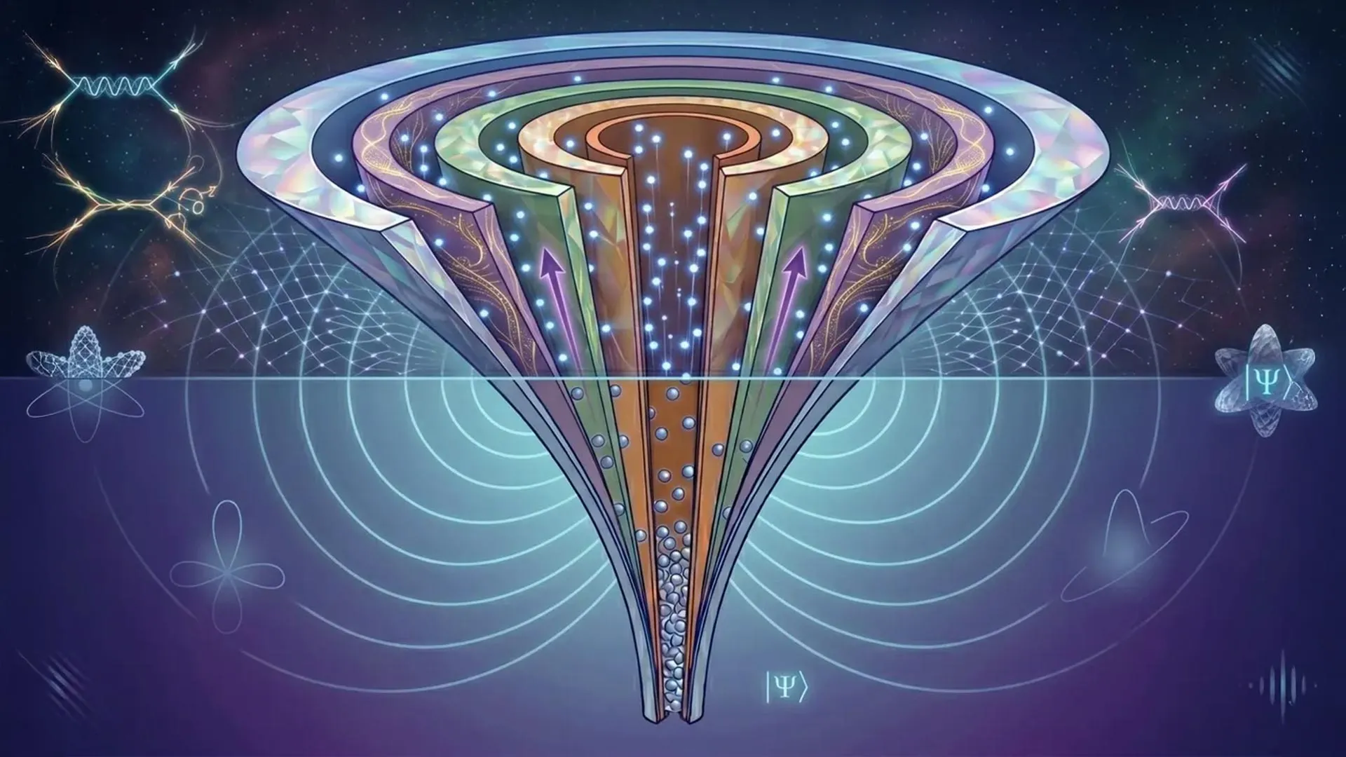
Following their theoretical proposal, the Peking University team published a subsequent paper in eLight detailing the experimental and physical mechanisms behind this confinement. They identified a new class of electromagnetic eigenmodes which they named "narwhal-shaped wavefunctions." The name is derived from the unique spatial profile of the electromagnetic field produced by these modes.
The narwhal-shaped wavefunction is characterized by two distinct mathematical behaviors occurring simultaneously. Close to the geometric singularity—the "horn" of the narwhal—the electromagnetic field undergoes a local power-law enhancement. This allows the field intensity to spike to extreme levels at a specific point. Simultaneously, moving away from the singularity, the field exhibits a global exponential decay. This "body" of the narwhal ensures that the light remains tightly trapped at the source and does not leak into the surrounding environment.
This dual-nature profile is what allows these wavefunctions to bypass traditional limits. By concentrating energy through power-law growth and containing it through exponential decay, the researchers created a "trap" for light that is far more effective than the Gaussian beams used in standard optics.
Experimental Validation and Record-Breaking Data
To prove the existence of these wavefunctions, the Peking University researchers designed and fabricated a three-dimensional singular dielectric resonator. This device was engineered to test whether light could be confined below the diffraction limit in all three spatial dimensions using only lossless materials.
The team employed near-field scanning optical microscopy (NSOM) to map the electromagnetic fields with nanometer precision. The results were startling and aligned almost perfectly with their 3D simulations. The key data points from the experiment included:
- Mode Volume: The system achieved an ultrasmall mode volume of approximately 5 × 10⁻⁷ λ³. This represents a level of confinement several orders of magnitude beyond the standard diffraction limit.
- Field Enhancement: The power-law growth at the singularity resulted in a massive concentration of energy within a volume of just a few cubic nanometers.
- Lossless Performance: Unlike plasmonic resonators, the dielectric singular resonator showed no significant thermal signature, confirming that the energy was being confined without being converted into heat.
These metrics represent a new world record for light confinement in dielectric systems, effectively proving that "singulonics" is a viable path for the future of nanophotonics.
The Singular Optical Microscope: A New Frontier in Imaging
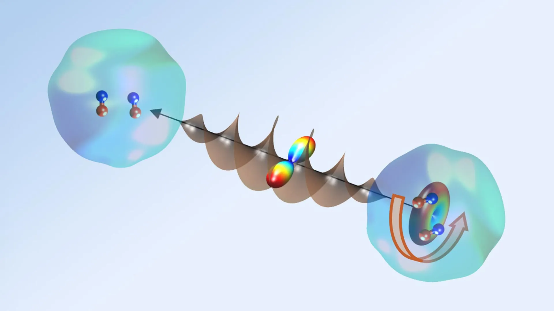
The practical utility of narwhal-shaped wavefunctions was immediately demonstrated through the invention of the "Singular Optical Microscope." Traditional optical microscopes are limited by the wavelength of light, typically unable to resolve features smaller than 200–300 nanometers. While techniques like Super-Resolution Microscopy (STED or PALM) exist, they often require complex fluorescent labeling or high-power lasers that can damage samples.
The singular optical microscope operates on a different principle. By exciting the singular eigenmodes within a dielectric cavity, the microscope creates a "nanosprobe" of light that is incredibly sensitive to its environment. When this localized field encounters a sub-wavelength structure, it causes a measurable shift in the resonance of the cavity.
In laboratory demonstrations, the Peking University team used this technique to achieve a spatial resolution of λ/1000. This allowed them to image deep-subwavelength patterns that would be invisible to any conventional optical system. The researchers successfully imaged the letters "PKU" (Peking University) and "SFM" (Scanning Force Microscopy) at scales previously reserved for electron microscopes. This suggests that the singular optical microscope could provide a non-destructive, label-free way to image biological molecules or semiconductor circuits at the atomic scale.
Chronology of the Singulonics Revolution
The development of this field has moved with remarkable speed, reflecting the significance of the findings:
- Pre-2020: Research focused heavily on All-Dielectric Nanophotonics, using Mie resonances to control light, but failing to reach the confinement levels of plasmonics.
- August 2024: Ren-Min Ma’s team publishes "Singular dispersion equation for extreme light confinement" in Nature, providing the mathematical proof that lossless dielectrics can confine light to the sub-nanometer scale.
- Late 2024: The team publishes further findings in eLight, introducing the "narwhal-shaped wavefunction" concept and demonstrating the singular optical microscope.
- Present: The term "Singulonics" is adopted by the scientific community to describe this new branch of physics, with labs globally beginning to explore singular geometries in silicon-on-insulator (SOI) platforms.
Broader Implications and Future Outlook
The rise of singulonics carries profound implications for several high-tech industries. The most immediate impact is expected in the semiconductor industry. As electronic chips reach the physical limits of silicon, "optical interconnects"—using light instead of electricity to move data between chip cores—have been proposed as the only way to continue increasing processing speeds. Until now, the size of optical components made this impractical. Singulonics provides the blueprint for "nanophotonic transistors" and waveguides that match the scale of electronic components.
Furthermore, the discovery has significant potential in the field of quantum optics. Quantum computing requires the strong interaction between single photons and single atoms or "artificial atoms" (quantum dots). The narwhal-shaped wavefunction’s ability to concentrate light into a tiny volume increases the probability of these interactions, which could lead to more stable and scalable quantum processors.
Industry analysts also point to the potential for ultra-efficient data centers. Currently, a massive amount of energy is wasted in the conversion between optical fiber signals and electronic server signals. If singulonics allows for all-optical processing at the microchip level, energy consumption in global communications could drop precipitously.
In summary, the work of Ren-Min Ma and his colleagues at Peking University has resolved a century-old tension between the physics of light and the requirements of miniaturization. By identifying the singular dispersion equation and the narwhal-shaped wavefunctions, they have moved photonics out of the "bulky" era and into the realm of the truly microscopic. Singulonics is no longer just a theoretical framework; it is a demonstrated reality that promises to redefine the limits of imaging, computing, and sensing in the 21st century.


Leave a Reply