
The global transition toward renewable energy has placed a significant spotlight on perovskite solar cells (PSCs), a technology that has evolved from a laboratory curiosity into a formidable contender for the future of photovoltaics. While silicon-based solar panels have dominated the market for decades, perovskites offer the promise of higher efficiency, lower manufacturing costs, and greater versatility. However, the path to commercialization has been hindered by challenges in scaling these cells from small, high-performance laboratory samples to large-area modules suitable for industrial use. In a major breakthrough, researchers from the Qingdao Institute of Bioenergy and Bioprocess Technology (QIBEBT) of the Chinese Academy of Sciences have developed a novel crystal-solvate (CSV) pre-seeding technique that addresses these hurdles. This advancement, detailed in the journal Nature Synthesis on February 27, provides a new pathway for creating stable, high-efficiency inverted perovskite solar modules.
The Evolution and Architecture of Perovskite Solar Cells
Perovskites are a class of materials characterized by a specific crystal structure, typically represented by the chemical formula ABX3. In the context of solar energy, organic-inorganic lead halide perovskites have shown an unprecedented rise in power conversion efficiency (PCE), jumping from under 4% in 2009 to over 26% in recent laboratory tests. This rapid progress is largely due to the material’s excellent light-harvesting capabilities, long charge-carrier diffusion lengths, and high defect tolerance.
Conventionally, PSCs are constructed in an "n-i-p" (normal-intrinsic-positive) configuration. In this setup, the electron transport layer (ETL) is deposited first, followed by the perovskite absorber and then the hole transport layer (HTL). While this architecture has yielded record-breaking efficiencies in small-scale cells, it often relies on dopants in the transport layers that can compromise the long-term stability of the device. Furthermore, the high-temperature processing often required for the ETL can limit the types of substrates used, such as flexible plastics.
In response, researchers have turned to "inverted" PSCs, or the "p-i-n" (positive-intrinsic-normal) structure. In an inverted cell, the positions of the transport layers are swapped, with the HTL placed underneath the perovskite layer. This design is inherently more compatible with tandem solar cell configurations (such as perovskite-silicon hybrids) and offers superior stability. Most importantly for industry, inverted cells are better suited for solution-based, large-area processing methods like slot-die coating or roll-to-roll manufacturing.
The Challenge of the Buried Interface
Despite their theoretical advantages, inverted PSCs have historically lagged behind their conventional counterparts in terms of peak efficiency. The primary bottleneck is found at the "buried interface"—the junction where the bottom of the perovskite layer meets the hole transport layer.
In many high-performance inverted cells, self-assembled monolayers (SAMs) are used as the HTL. While SAMs are excellent for aligning energy levels and facilitating hole extraction, they are often hydrophobic (water-repelling). When a liquid perovskite precursor is applied over these surfaces, it can struggle to spread uniformly. This poor wetting leads to microscopic structural irregularities, voids, and electronic defects at the interface. These hidden flaws act as recombination centers, where charge carriers are lost before they can be harvested as electricity, thereby reducing both the initial efficiency and the operational lifespan of the device.
Controlling the growth of the perovskite crystal from the bottom up is notoriously difficult because the interface is obscured as soon as the film begins to form. Previous attempts to fix this have involved post-treatment of the film or the use of various additives, but these often fail to address the root cause: the chaotic nature of nucleation and crystal growth at the initial contact point.
The CSV Pre-Seeding Solution
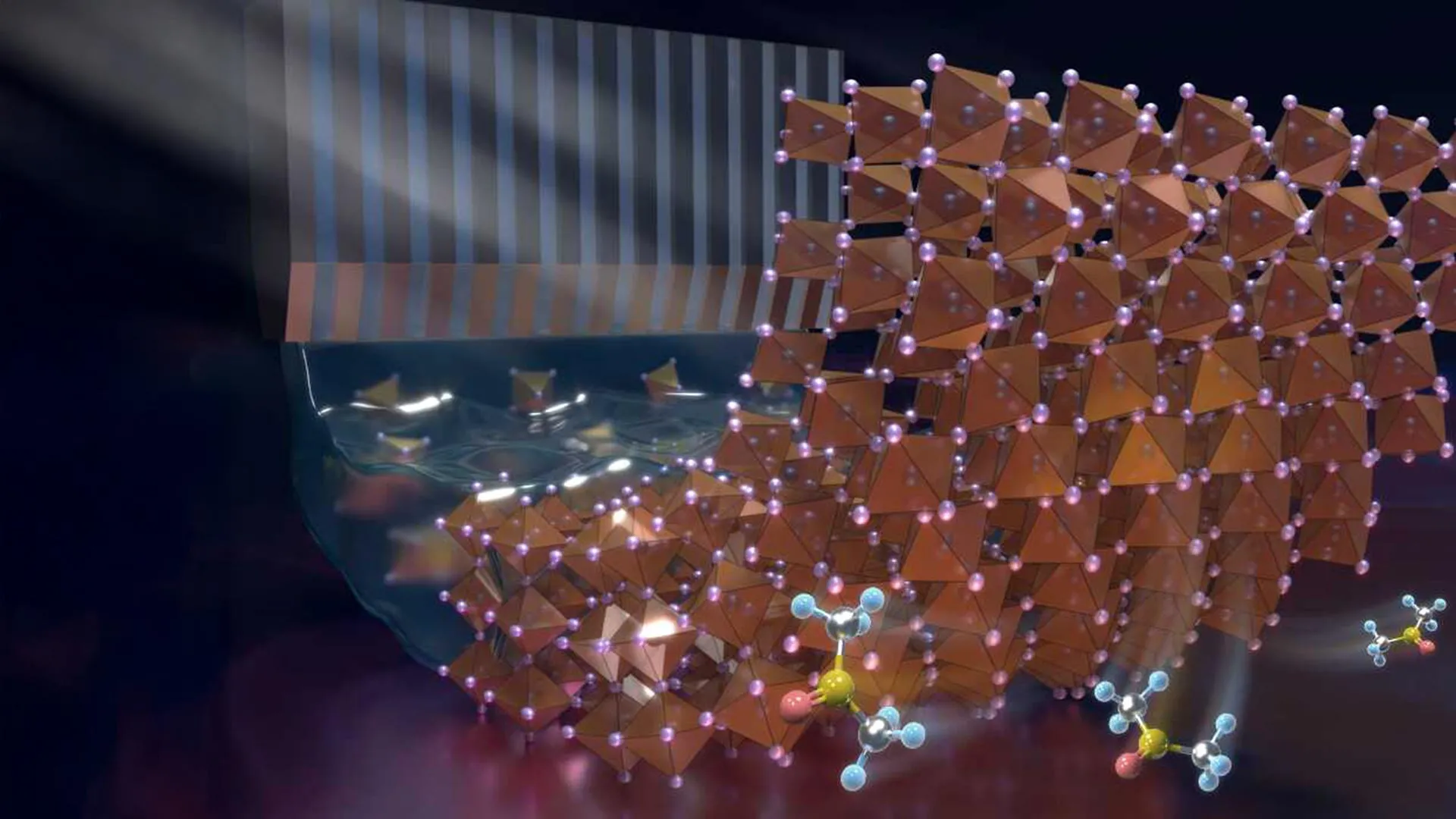
The research team at QIBEBT, led by Professor Shuping Pang and Dr. Xiuhong Sun, introduced a sophisticated strategy to regain control over this buried interface. Their method involves the use of crystal-solvate (CSV) pre-seeding.
The process begins with the deposition of specially engineered low-dimensional halide crystal-solvate seeds onto the SAM-modified substrate. These seeds have the chemical formula $PDPbI_4 cdot DMSO$. By applying these nanocrystals before the main perovskite layer is formed, the researchers create a structural template that dictates how the subsequent crystals grow.
The CSV nanocrystals are rod-shaped, providing a physical framework that improves the spread of the perovskite precursor across the hydrophobic SAM surface. This ensures that the entire substrate is covered uniformly, eliminating the "beading" effect that often occurs with standard coating methods. Once the main perovskite precursor is applied, these pre-deposited nanocrystals serve as a multitude of nucleation sites. Instead of crystals forming randomly and clumping together, they grow in an organized, directed manner from the seeds upward.
Lattice-Confined Solvent Annealing: A Dual-Action Strategy
One of the most innovative aspects of the QIBEBT study is the role of dimethyl sulfoxide (DMSO) within the CSV structure. In standard perovskite fabrication, solvent molecules are often removed quickly during a process called anti-solvent dripping or thermal annealing. However, in the CSV method, the DMSO is chemically embedded within the seed crystals.
During the thermal annealing stage—where the film is heated to finalize its crystal structure—the DMSO molecules are released gradually from the seeds. The researchers refer to this as "lattice-confined solvent annealing" (LCSA). This slow release creates a localized, solvent-rich micro-environment right at the buried interface.
This LCSA process serves two vital functions. First, it provides the necessary "mobility" for the growing perovskite grains to rearrange themselves into a more perfect, dense structure. Second, it acts as a restorative agent, filling in the microscopic grooves and boundary gaps that typically form at the bottom of the film. The result is a perovskite "bottom layer" that is highly oriented, dense, and remarkably free of the voids that usually plague inverted cells.
Breaking the Scaling Bottleneck: From Cells to Modules
The true test of any solar technology is its performance at scale. In the laboratory, researchers often use "spin-coating," a technique that produces high-quality films but wastes significant amounts of material and is limited to very small areas (typically less than 1 $cm^2$). To transition to the factory floor, technologies must work with continuous coating methods like "slot-die coating."
Scaling usually comes with a significant "size effect" penalty—as the area of the solar cell increases, the efficiency typically drops sharply due to increased resistance and non-uniformity in the film. The QIBEBT team applied their CSV pre-seeding method to a slot-die coating process to fabricate a perovskite solar mini-module.
The results were record-setting for this architecture. The mini-module, which featured an aperture area of 49.91 $cm^2$, achieved a certified power conversion efficiency of 23.15%. Crucially, the efficiency drop from their small-scale laboratory cells to this much larger module was less than 3%. This minimal "scaling loss" is one of the lowest ever reported in perovskite research, suggesting that the CSV method effectively neutralizes the traditional barriers to large-area manufacturing.
Technical Data and Stability Metrics
The structural improvements at the buried interface translated directly into enhanced physical durability. The researchers subjected the devices to rigorous testing to simulate real-world conditions.
- Efficiency: Small-area cells using the CSV method reached efficiencies exceeding 25%, while the ~50 $cm^2$ module maintained 23.15%.
- Structural Integrity: Scanning Electron Microscopy (SEM) and X-ray diffraction (XRD) confirmed a significantly higher degree of crystallinity and a reduction in interfacial voids compared to control samples.
- Thermal and Light Stability: By eliminating the defects at the buried interface that often act as triggers for degradation, the cells showed improved resistance to heat and light-induced stress. Under continuous illumination, the devices retained the vast majority of their initial efficiency over hundreds of hours of testing.
Expert Perspectives and Industry Impact
Dr. Xiuhong Sun, co-first author of the study, highlighted the importance of addressing the hidden layers of the cell. "We have developed an integrated approach that simultaneously addresses crystallization regulation and interface stabilization," Dr. Sun stated. "This strategy delivers good performance even at buried interfaces, which are notoriously challenging to precisely control."
Professor Shuping Pang emphasized the broader potential of this discovery. "This technology overcomes the longstanding scaling bottleneck caused by size effects through the combination of induced crystallization and buried interface restoration," Pang said. He noted that the CSV concept isn’t limited to a single type of perovskite. By swapping out different organic cations and solvent molecules, researchers can create a "diverse library" of CSV materials.
This flexibility suggests that the CSV pre-seeding technique could become a standard tool in the field of "soft-lattice" semiconductors, which includes not only solar cells but also light-emitting diodes (LEDs) and photodetectors.
Future Outlook: The Path to Commercialization
The success of the QIBEBT team comes at a critical time for the solar industry. As traditional silicon cells approach their theoretical efficiency limit (the Shockley-Queisser limit), the industry is looking for "Silicon-Plus" solutions. Perovskite-silicon tandem cells are the most likely candidate for the next generation of commercial solar panels. Because the CSV method works so well with inverted architectures—the preferred top-cell for tandems—this research could accelerate the timeline for these ultra-high-efficiency panels to reach the market.
However, challenges remain. The industry must still prove that perovskite modules can last for 20 to 25 years in harsh outdoor environments, a standard set by silicon. While the CSV method improves stability by cleaning up the buried interface, further research into encapsulation and the mitigation of lead toxicity will be essential.
The work at QIBEBT represents a shift in focus from simply chasing record efficiencies to solving the practical engineering problems of mass production. By mastering the buried interface, the researchers have moved the industry one step closer to a future where high-efficiency, low-cost perovskite solar power is a cornerstone of the global energy grid.


Leave a Reply