

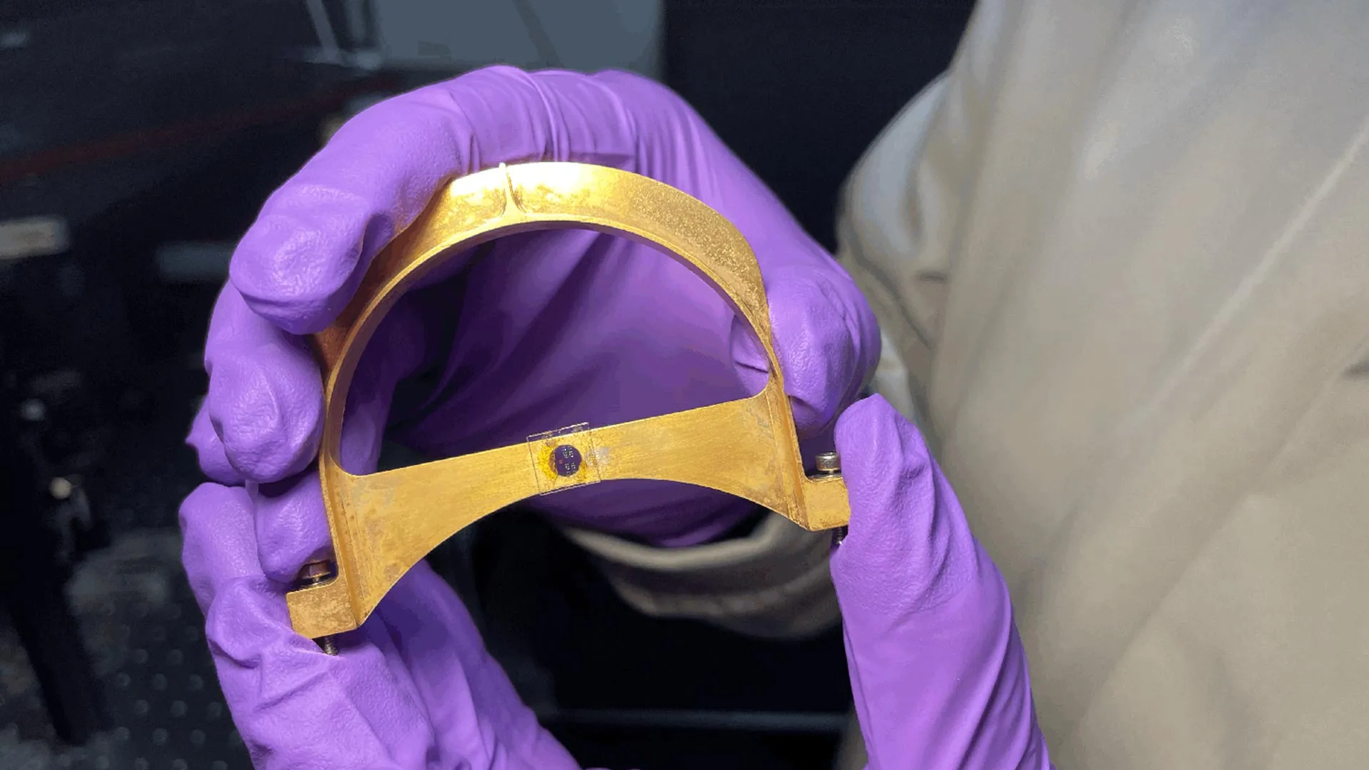
In a significant departure from the ultra-cold environments typically required for quantum operations, a team of researchers at Stanford University has successfully demonstrated a room-temperature interface between light and matter at the nanoscale. The development, centered on a device that links the quantum properties of photons and electrons without the need for cryogenic cooling, represents a potential paradigm shift in the field of quantum information science. By utilizing a combination of transition metal dichalcogenides (TMDCs) and nanopatterned silicon, the researchers have created a stable spin connection that could eventually allow quantum technologies to move out of specialized laboratories and into everyday consumer electronics.
For decades, the primary hurdle to the scalability of quantum computing has been the requirement for extreme temperatures. Most current quantum systems rely on superconducting qubits or trapped ions that must be kept at temperatures near absolute zero—approximately -459 degrees Fahrenheit or 0 Kelvin. These temperatures are necessary to prevent decoherence, a process where the surrounding thermal energy disrupts the fragile quantum states of superposition and entanglement. The Stanford team’s new device bypasses this requirement, operating efficiently at ambient temperatures and offering a more practical pathway toward a global quantum internet.
The Architecture of the Nanoscale Device
The breakthrough rests on the innovative pairing of two distinct materials: molybdenum diselenide (MoSe2) and a silicon substrate. Molybdenum diselenide is a member of the transition metal dichalcogenide family, a class of "2D materials" that are only a few atoms thick. These materials have gained significant attention in the scientific community for their unique optical and electronic properties, particularly their ability to host "excitons"—bound states of an electron and an electron hole that can interact strongly with light.
The researchers layered a thin film of MoSe2 onto a silicon base that had been etched with precise, nanoscale patterns. These patterns are engineered to be roughly the size of the wavelength of visible light, making them invisible to the naked eye but highly influential on the behavior of photons. The primary function of the silicon nanostructures is to manipulate the geometry of incoming light, transforming standard photons into what the researchers call "twisted light."
"The silicon nanostructures enable what we call ‘twisted light,’" explains Feng Pan, a postdoctoral scholar in the lab of Jennifer Dionne and the paper’s first author. "The photons spin in a corkscrew fashion, but more importantly, we can use these spinning photons to impart spin on electrons that are the heart of quantum computing."
The Mechanics of Twisted Light and Electron Spin
In quantum mechanics, "spin" is an intrinsic form of angular momentum carried by elementary particles. For a quantum communication system to function, there must be a reliable way to transfer information between light (which carries data over distances) and matter (which stores and processes data). This is typically achieved through entanglement, a phenomenon where the quantum states of two particles become linked, such that the state of one instantly influences the state of the other.
The Stanford device achieves this by using the "twisted" photons to influence the spin of electrons within the molybdenum diselenide layer. As the photons interact with the material, their corkscrew motion dictates the direction of the electron spin, creating a robust coupling. This interaction is facilitated by the silicon nanostructures, which confine the light into a very small volume, increasing the intensity of the interaction and allowing it to persist even at room temperature.
Jennifer Dionne, a professor of materials science and engineering at Stanford and the study’s senior author, notes that while the materials used are known to science, the application is revolutionary. "The material in question is not really new, but the way we use it is," Dionne says. "It provides a very versatile, stable spin connection between electrons and photons that is the theoretical basis of quantum communication. Typically, however, the electrons lose their spin too quickly to be useful."
Overcoming the Decoherence Barrier
The significance of achieving this at room temperature cannot be overstated. In traditional quantum setups, the energy from room-temperature vibrations (phonons) is enough to "flip" an electron’s spin or destroy a photon’s phase, leading to the loss of information. To combat this, researchers have historically used dilution refrigerators, which are massive, power-hungry, and cost hundreds of thousands of dollars to operate.
By engineering a device that maintains spin stability through geometric manipulation of light rather than brute-force cooling, the Stanford team has lowered the barrier to entry for quantum research. The device’s compact design is not only more affordable but also more resilient. The use of silicon is particularly strategic; because silicon is the foundational material of the modern semiconductor industry, the device could potentially be manufactured using existing fabrication techniques, facilitating a smoother transition from laboratory prototype to industrial product.
Chronology of Development and Collaborative Research
The development of this device is the result of years of interdisciplinary collaboration at Stanford. The project drew on the expertise of several prominent researchers, including Fang Liu and Tony Heinz, who are specialists in the physics of 2D materials.
The timeline of the research follows a trajectory of increasing precision in nanofabrication:
- Phase I (Conceptualization): Identifying TMDCs as a candidate for room-temperature quantum interfaces due to their strong light-matter coupling.
- Phase II (Design): Engineering the silicon nanopatterns to create specific optical chiralities (twisted light).
- Phase III (Integration): Successfully layering MoSe2 onto the patterned silicon without damaging the atomic structure of the 2D material.
- Phase IV (Validation): Measuring the spin-transfer efficiency at room temperature and confirming entanglement between the optical and electronic states.
"It all comes down to this material and our silicon chip," Pan says. "Together, they efficiently confine and enhance the twisting of light to create a strong coupling of spin between photons and electrons. This stabilizes the quantum state that makes quantum communication possible."
Economic and Industrial Implications
The move toward room-temperature quantum components has profound implications for the global economy and the future of technology. Currently, the "Quantum Race" is dominated by nations and corporations capable of sustaining the massive infrastructure required for cryogenic computing. If quantum components can be miniaturized and operated at ambient temperatures, the landscape of the industry changes entirely.
Secure Communications: Quantum Key Distribution (QKD) relies on the fact that any attempt to eavesdrop on a quantum signal changes its state, alerting the users. A room-temperature device could allow for secure quantum encryption modules to be installed in standard telecommunications racks, protecting financial and governmental data from future quantum-based hacking.
Advanced Sensing: The sensitivity of quantum states to their environment makes them excellent sensors. Room-temperature quantum sensors could be used in medical imaging, allowing for MRI-like detail at a fraction of the size and cost, or in geology for detecting mineral deposits or seismic activity.
Artificial Intelligence: Quantum-enhanced machine learning algorithms require high-speed data transfer between classical and quantum processors. This device provides a bridge that could facilitate the "quantum-classical" hybrid systems necessary for the next generation of AI.
Technical Analysis: The Path to Miniaturization
While the Stanford device is a major milestone, the researchers acknowledge that a fully functional "quantum cell phone" is still a distant goal. The current device is a single component—a qubit interface. A complete system would require the integration of several other room-temperature components, including:
- Single-photon sources: To provide the individual light particles needed for entanglement.
- Quantum modulators: To encode information onto the twisted light.
- Detectors: To read the quantum state at the end of the transmission.
- Interconnects: To link multiple nanoscale devices into a coherent network.
The team is currently exploring other TMDC materials, such as tungsten diselenide (WSe2), to see if they offer even longer spin coherence times. They are also investigating "valleytronics," a field of electronics that uses the "valley" index of electrons in certain crystals to store information, which could work in tandem with their spin-based system.
Broader Impact and Future Outlook
The research, published in Nature Communications, arrives at a time when the United States and other global powers are increasing investment in quantum infrastructure. The U.S. National Quantum Initiative Act, for instance, emphasizes the need for "plug-and-play" quantum components that can integrate with existing fiber-optic networks.
By proving that light and matter can be entangled at room temperature in a silicon-compatible format, the Stanford team has provided a blueprint for the "democratization" of quantum technology. If these devices can be scaled, the requirement for liquid helium and massive cooling towers will vanish, allowing quantum processors to be integrated into data centers, autonomous vehicles, and eventually, handheld devices.
"If we can do that, maybe someday we could do quantum computing in a cell phone," Pan says. "But that’s a 10-plus-year plan."
The road ahead involves rigorous testing of the device’s durability and the optimization of the spin-transfer efficiency. However, the foundational discovery—that twisted light can stabilize quantum information at room temperature—stands as a critical bridge between the theoretical potential of quantum mechanics and the practical realities of modern engineering. As researchers continue to refine these nanoscale structures, the goal of a practical, accessible quantum network moves closer to reality, promising a future of unprecedented computational power and communication security.



















Leave a Reply