

A multidisciplinary team of researchers at the University of California, Davis, has documented a significant physical phenomenon in a class of materials known as halide perovskites, revealing that these crystals undergo rapid and reversible structural changes when exposed to light. The study, published in the journal Advanced Materials on March 3, identifies a "photostriction" effect that allows the material’s atomic lattice to expand or contract upon illumination before returning to its original state once the light source is removed. This discovery challenges the traditional understanding of semiconductor behavior and suggests a future where electronic devices can be controlled via optical stimuli rather than conventional electrical signals.
The research, led by Marina Leite, a professor of materials science and engineering at UC Davis, highlights the "smart" nature of perovskites. Unlike silicon, which has dominated the semiconductor industry for decades due to its stability and predictability, perovskites offer a level of flexibility and tunability that could redefine the boundaries of optoelectronics. The findings represent a major step forward in the development of switchable photonic devices, light-driven sensors, and advanced actuators, potentially reducing the energy consumption and complexity of next-generation hardware.
The Atomic Architecture of Perovskites
To understand the significance of this discovery, it is necessary to examine the unique chemical and structural composition of perovskites. While the term "perovskite" originally referred to a specific mineral (calcium titanate), it now describes a broad class of compounds that share a specific crystal structure known as ABX3. In this arrangement, the "A" and "B" represent cations of different sizes, and "X" represents an anion that bonds to both.
At the microscopic level, the perovskite structure is characterized by a central atom (B) surrounded by an octahedron of six atoms (X), resembling two pyramids joined at their bases. This entire unit is nested within a larger cube, with atoms (A) occupying each corner. This specific geometry allows for an incredible variety of elemental combinations, including organic-inorganic hybrids. This flexibility is what allows scientists to "tune" the material, adjusting its bandgap—the energy required for electrons to move and conduct electricity—by simply altering its chemical makeup.
Historically, perovskites gained massive scientific attention in the late 2000s for their potential in photovoltaic cells. Since 2009, the power conversion efficiency of perovskite solar cells has skyrocketed from under 4% to over 25%, a rate of improvement unseen in any other material class. However, the UC Davis study shifts the focus from how these materials absorb energy to how they physically react to it, revealing a mechanical response that mimics biological systems.
Chronology of the Discovery and Experimental Design
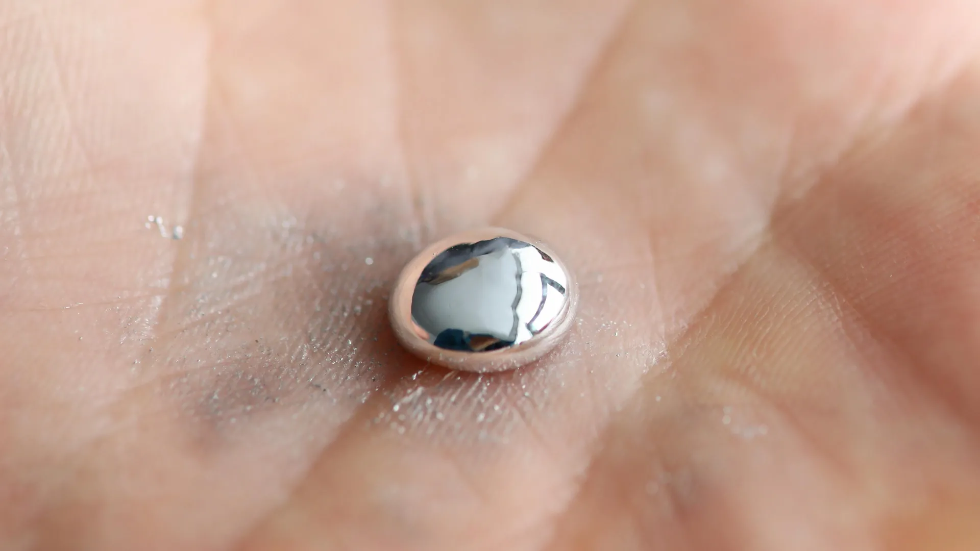
The path to this discovery involved a collaborative international effort and the use of high-precision characterization tools. The research timeline began with the synthesis of high-quality halide perovskite crystals by a team of collaborators at ETH Zürich in Switzerland, including Bekir Turedi, Andrii Kanak, and Professor Maksym Kovalenko. These crystals were then transported to the UC Davis Advanced Materials Characterization and Testing (AMCaT) laboratory for rigorous analysis.
Mansha Dubey, a graduate student in Leite’s lab and the lead researcher on the project, designed an experiment to observe the material’s atomic response in real-time. The team utilized a combination of laser stimulation and X-ray diffraction (XRD) measurements. By directing a laser at the crystal lattice and simultaneously measuring the diffraction patterns of X-rays passing through the material, the researchers could track the movement of atoms with sub-angstrom precision.
The experiments were conducted under varying conditions of light intensity and wavelength. The team observed that as soon as the laser hit the crystal, the internal lattice shifted. This was not a permanent deformation or a thermal expansion caused by heat, but a direct response to the photons interacting with the electronic structure of the material. Most notably, the researchers documented that the process was fully reversible. When the laser was deactivated, the atoms snapped back into their original positions within milliseconds.
Supporting Data: The Photostriction Effect and Tunability
The data collected by Leite and her team demonstrate that halide perovskites exhibit a photostriction effect that is markedly different from the behavior of traditional semiconductors like silicon or gallium arsenide. In silicon, the crystal lattice remains largely rigid under light exposure; any changes are typically the result of thermal expansion, which is slow and can lead to material fatigue over time.
In contrast, the perovskite response is "elastic" and highly sensitive to the properties of the light source. The study found that the magnitude of the lattice shift is not a simple binary "on/off" state. Instead, it functions more like a dimmer switch. The intensity of the light—the number of photons hitting the surface—directly correlates with the degree of structural change. Furthermore, the color (wavelength) of the light also plays a crucial role. If the light frequency is above the material’s bandgap, the response is significantly more pronounced.
This tunability is a cornerstone of the research. By adjusting the chemical composition of the halide perovskite—for example, by swapping out lead for tin or changing the halide from iodine to bromine—the researchers can pre-determine which specific wavelength of light will trigger the shape change. This allows for the creation of materials that are "programmed" to respond only to specific parts of the electromagnetic spectrum.
Strategic Funding and Industrial Implications
The implications of this research extend beyond the laboratory, as evidenced by the entities funding the project. The study was supported by the Defense Advanced Research Projects Agency (DARPA) under a program focused on developing materials for switchable photonic devices. DARPA’s interest suggests that light-controlled perovskites could have significant applications in national security and telecommunications, particularly in creating high-speed optical switches that do not rely on bulky electronic components.
Additional funding was provided by the National Science Foundation (NSF), which also supported the establishment of the AMCaT facility at UC Davis. The involvement of these federal agencies underscores the strategic importance of finding alternatives to silicon. As the semiconductor industry approaches the physical limits of Moore’s Law, the ability to control materials with light rather than electricity offers a potential pathway to bypass the heat and speed bottlenecks inherent in traditional microchips.
From an economic perspective, perovskites offer a distinct advantage: they can be manufactured using solution-processing techniques, such as inkjet printing or spin-coating, at much lower temperatures than the high-heat processes required for purified silicon. The discovery of photostriction adds a new layer of value to these materials, transforming them from mere energy absorbers into active components for mechanical and optical systems.
Expert Analysis of Broader Impacts
The ability to control a material’s shape via light opens the door to a new generation of "wireless" technology. In current electronic systems, actuators—the components responsible for moving or controlling a mechanism—require wires to deliver electricity. A perovskite-based actuator could theoretically be controlled by a remote laser or LED, eliminating the need for complex wiring and reducing the weight of the device.
"This is a unique phenomenon that you don’t see with traditional semiconductors," Professor Leite noted during the announcement of the findings. She emphasized that the chemistry of perovskites allows for the creation of devices that were previously impossible to build. By leveraging the photostriction effect, engineers could develop sensors that detect specific light signatures by physically expanding to complete a circuit, or optical buffers that slow down light by changing the physical path it must travel.
However, challenges remain. While the reversibility of the shape change is a breakthrough, the long-term stability of halide perovskites is still a subject of intense research. These materials can be sensitive to moisture and oxygen, which can lead to degradation over time. The UC Davis team’s work provides a framework for understanding how to stabilize these structures while maintaining their "smart" properties.
Conclusion and Future Outlook
The research published in Advanced Materials marks a pivot point in the study of halide perovskites. By identifying and quantifying the reversible photostriction effect, the UC Davis team has provided a blueprint for the design of light-responsive materials. The transition from electricity-controlled to light-controlled devices could lead to faster, more efficient, and more versatile technology across a range of industries, from aerospace to consumer electronics.
As the team continues to explore the limits of these materials, the focus will likely shift toward integrating these crystals into functional micro-devices. The collaboration between UC Davis and ETH Zürich demonstrates the importance of international cooperation in solving fundamental problems in materials science. For now, the discovery that a simple beam of light can reshape a crystal lattice provides a compelling glimpse into a future where the boundary between light and matter becomes increasingly fluid.
The successful demonstration of this "dimmer-like" response suggests that the next generation of semiconductors will not just be faster, but also more adaptable, responding to the environment in ways that silicon never could. With the support of DARPA and the NSF, the researchers at UC Davis are positioned at the forefront of a movement that may eventually see perovskites move from the laboratory into the core of the world’s most advanced technological systems.


Leave a Reply