

The global energy landscape is currently undergoing a radical transformation as researchers seek more efficient, cost-effective alternatives to traditional silicon-based solar technology. For decades, silicon has reigned supreme, largely because it can be refined to near-perfect crystalline purity, allowing electrical charges to move without interruption. However, a relatively new class of materials known as lead-halide perovskites has challenged this dominance, achieving comparable efficiency levels despite being riddled with structural flaws and impurities. A new study published in the journal Nature Communications by researchers at the Institute of Science and Technology Austria (ISTA) has finally unraveled the physical mechanism behind this "defect tolerance," identifying internal structural networks that act as high-speed "highways" for electrical charges.
This discovery addresses a fundamental paradox in materials science: how a material produced through low-cost, solution-based methods—often resulting in a "messy" internal structure—can outperform highly engineered, ultra-pure semiconductors. The findings by Dmytro Rak and Zhanybek Alpichshev suggest that the secret to the success of perovskites lies not in the elimination of defects, but in the way these defects are organized. By understanding this internal architecture, the scientific community may finally be able to transition perovskite solar cells from laboratory curiosities to a cornerstone of the global renewable energy infrastructure.
The Evolution of Perovskite Research: A Chronological Overview
The history of perovskites dates back to 1839, when the mineral calcium titanate was discovered in the Ural Mountains by Gustav Rose and named after Russian mineralogist Lev Perovski. While the term originally referred to that specific mineral, it now describes a broad class of compounds that share the same $ABX_3$ crystal structure.
The timeline of lead-halide perovskites specifically is a journey from obscurity to the forefront of optoelectronics:
- 1970s: Lead-halide perovskites were first synthesized and characterized. At the time, they were viewed primarily as academic curiosities with interesting structural properties but little perceived practical application in electronics.
- 2009: A breakthrough occurred when Tsutomu Miyasaka and his team at Toin University of Yokohama used perovskites as light-sensitizers in a solar cell, achieving an initial efficiency of roughly 3.8%.
- 2012: Research accelerated as scientists discovered that perovskites could function as solid-state light absorbers. Efficiency plummeted past 10% in just a few years, a rate of improvement never before seen in the history of photovoltaics.
- 2015–2020: Perovskites began to show promise beyond solar cells, appearing in high-definition LEDs, X-ray detectors, and quantum computing research. Efficiency records for perovskite-silicon "tandem" cells began to approach the 30% mark.
- 2024: The ISTA study provides the first comprehensive physical explanation for how these materials manage charge transport, solving the "mystery of efficiency" that has persisted for over a decade.
Understanding the Charge Transport Challenge
To appreciate the significance of the ISTA discovery, one must understand the basic physics of a photovoltaic cell. When sunlight hits a solar cell, the energy from the photons excites electrons, moving them to a higher energy state. This creates a "hole"—a positively charged vacancy—where the electron used to be. For electricity to be generated, these negatively charged electrons and positively charged holes must be separated and moved to opposite electrodes.
In a perfect crystal, this journey is straightforward. However, in most materials, defects act as "traps." If an electron encounters a structural flaw, it may lose its energy and recombine with a hole, a process that generates heat instead of electricity. Silicon solar cells solve this by being "perfect"; they are manufactured in cleanrooms to ensure that almost no defects exist to trap charges.
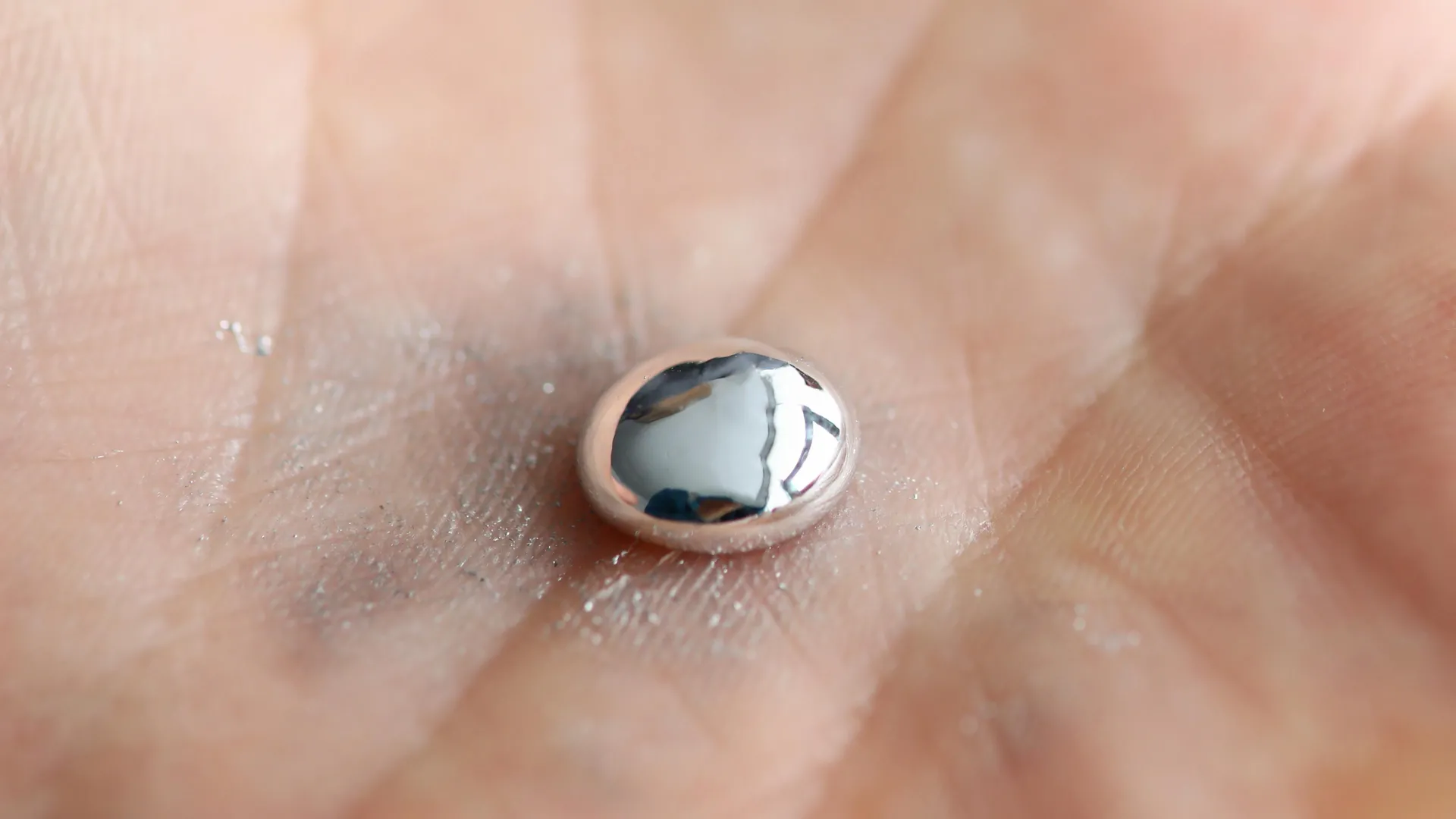
Lead-halide perovskites, by contrast, are "dirty" materials. They are often printed or spun from liquid solutions, leading to a landscape of structural irregularities. On a microscopic scale, an electron in a perovskite cell must travel the equivalent of hundreds of kilometers without being trapped. Until now, scientists could not explain why these charges didn’t simply vanish into the material’s many flaws.
The ISTA Study: Visualizing Internal "Highways"
The research team at ISTA, led by Dmytro Rak and Zhanybek Alpichshev, suspected that the material’s internal structure was actively assisting charge separation rather than hindering it. To prove this, they utilized nonlinear optical techniques to inject charges deep within the bulk of a perovskite crystal, far from the surface where measurements are typically taken.
The team observed a consistent phenomenon: even without an external power source or voltage, the charges always flowed in a specific direction. This indicated the presence of a powerful, naturally occurring internal electric field. "Our observation clearly indicated that even deep inside single crystals of unmodified, as-grown perovskites, there are internal forces that separate opposite charges," noted Alpichshev.
To locate where these forces were coming from, the researchers focused on "domain walls." These are thin regions where the orientation of the crystal structure shifts slightly. While previously thought to be minor imperfections, the ISTA team hypothesized that these walls were the key to the material’s efficiency.
Innovations in Microscopic Visualization
Confirming the existence of these internal networks required a creative leap in imaging technology. Standard microscopes cannot see deep into a crystal, and many advanced probes only interact with the surface. Dmytro Rak developed a novel technique that he compares to medical angiography, where a contrast dye is injected into a patient’s bloodstream to visualize arteries.
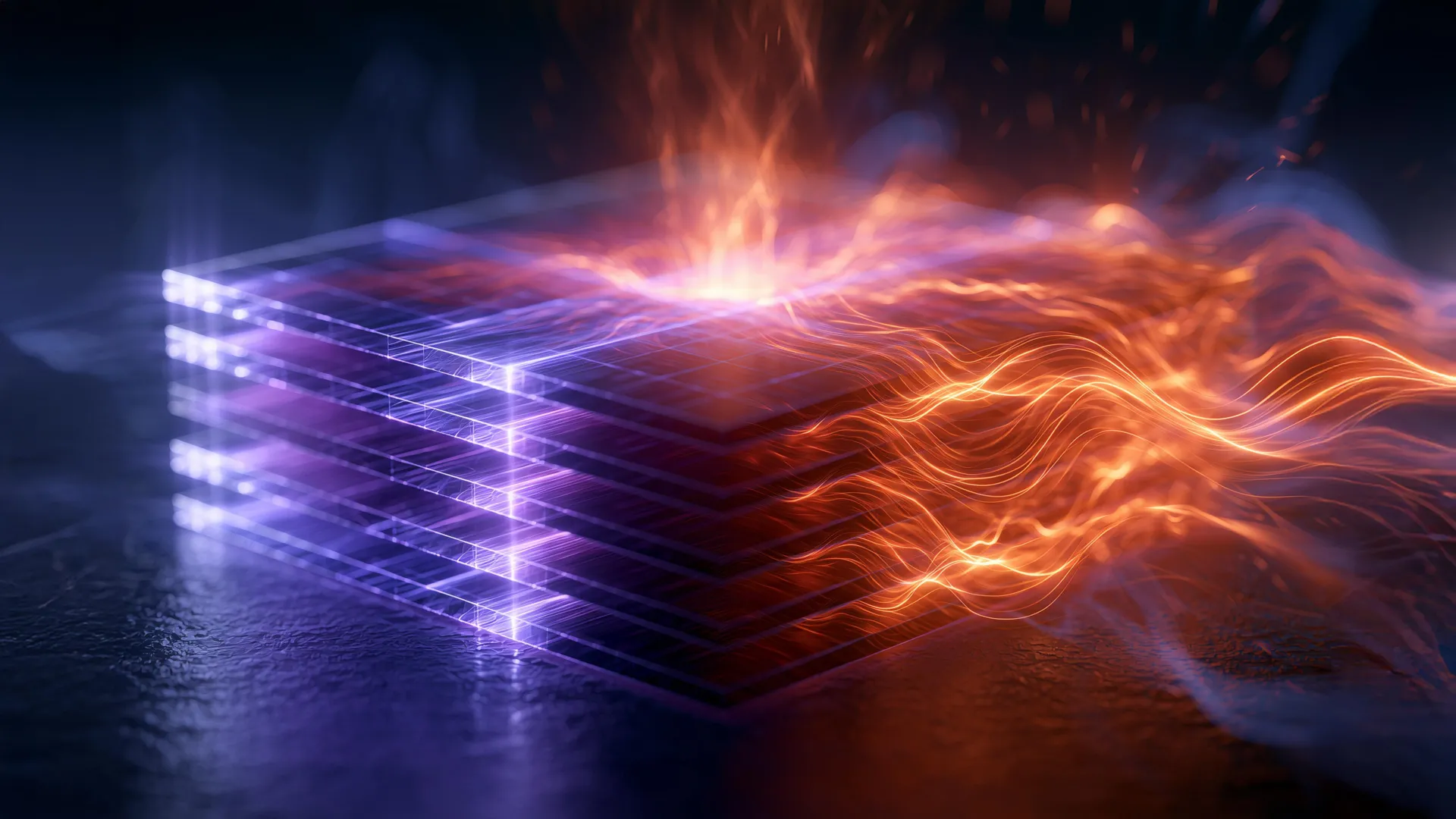
In the ISTA experiment, Rak introduced silver ions into the perovskite. Because the material is an ionic conductor, the silver ions migrated through the crystal. Crucially, they accumulated specifically along the domain walls. Once the ions were chemically converted into metallic silver, they formed a visible map of the internal structure. Under the microscope, a dense, interconnected network of "highways" appeared, stretching throughout the entire volume of the material.
The data revealed that when light creates an electron-hole pair near one of these domain walls, the local electric field pulls the two charges apart. The electron stays on one side of the wall, and the hole stays on the other. Because they are physically separated by the wall, they cannot recombine. They are then free to slide along the wall—the "highway"—until they reach the electrodes.
Supporting Data and Comparative Analysis
The implications of this discovery are supported by the rapid rise in perovskite efficiency metrics. According to the National Renewable Energy Laboratory (NREL), perovskite solar cell efficiency has climbed from under 4% in 2009 to over 26% in 2024. In comparison, silicon took nearly 40 years to achieve a similar jump in performance.
| Material | Efficiency (2009) | Efficiency (2024) | Manufacturing Complexity |
|---|---|---|---|
| Crystalline Silicon | ~25% | ~27% | High (Czochralski process, 1400°C) |
| Lead-Halide Perovskite | 3.8% | 26.1% | Low (Solution-based, <200°C) |
| Perovskite/Silicon Tandem | N/A | 33.9% | Moderate |
The ISTA study provides the theoretical framework that explains this data. It suggests that perovskites have a high "Shockley-Queisser limit" potential because their internal architecture minimizes the energy loss typically associated with non-perfect crystals.
Industry Reactions and Theoretical Impact
The scientific community has reacted to the ISTA findings with cautious optimism. For years, the "defect tolerance" of perovskites was a debated theory. Some researchers argued it was due to the heavy atoms like lead providing a unique screening effect, while others pointed to the material’s high dielectric constant. The ISTA work provides a unifying theory that accounts for these observations while placing the focus on the structural domain walls.
"With this comprehensive picture, we are finally able to reconcile many previously conflicting observations about lead-halide perovskites," says Rak. This sentiment is echoed by materials scientists who have struggled to explain why "messy" manufacturing processes often result in better-performing cells.
By identifying domain walls as the primary drivers of efficiency, the research suggests that the next phase of solar development should move away from purely chemical adjustments. Instead, the focus may shift toward "strain engineering"—manipulating the physical stress within the crystal to create more or better-organized domain walls, thereby increasing the density of the charge highways.
Broader Implications for Green Energy
The potential impact of this research on the global energy transition is significant. Current silicon manufacturing is energy-intensive and requires massive capital investment in specialized foundries. Perovskites, however, can be manufactured using techniques similar to newspaper printing—roll-to-roll processing—which could drastically lower the cost of solar energy.
Furthermore, the discovery of these "charge highways" may lead to advancements in other fields:
- Flexible Electronics: Because perovskites work well even when they aren’t perfect crystals, they can be applied to flexible plastics, allowing for solar-powered clothing, tents, or curved building surfaces.
- Medical Imaging: The high charge-collection efficiency makes perovskites excellent candidates for low-dose X-ray detectors, potentially reducing radiation exposure for patients.
- Quantum Coherence: As Alpichshev noted, these materials exhibit quantum properties at room temperature. The domain wall networks might offer a stable environment for quantum states, which is usually only possible at near-absolute zero temperatures.
Despite the excitement, challenges remain. Lead-halide perovskites contain lead, which poses environmental risks if the cells are damaged or improperly disposed of. Additionally, the very "messiness" that allows for charge highways also makes the materials susceptible to degradation from moisture and heat.
However, the ISTA study provides the roadmap needed to address these issues. By understanding the internal mechanics of the material, engineers can now design protective coatings and chemical stabilizers that preserve the domain wall networks. As the industry moves toward commercialization, the transition from silicon to perovskite—or the integration of both in tandem cells—looks increasingly inevitable. The resolution of this long-standing mystery marks a pivotal moment in the quest for a sustainable, high-efficiency solar future.


Leave a Reply