
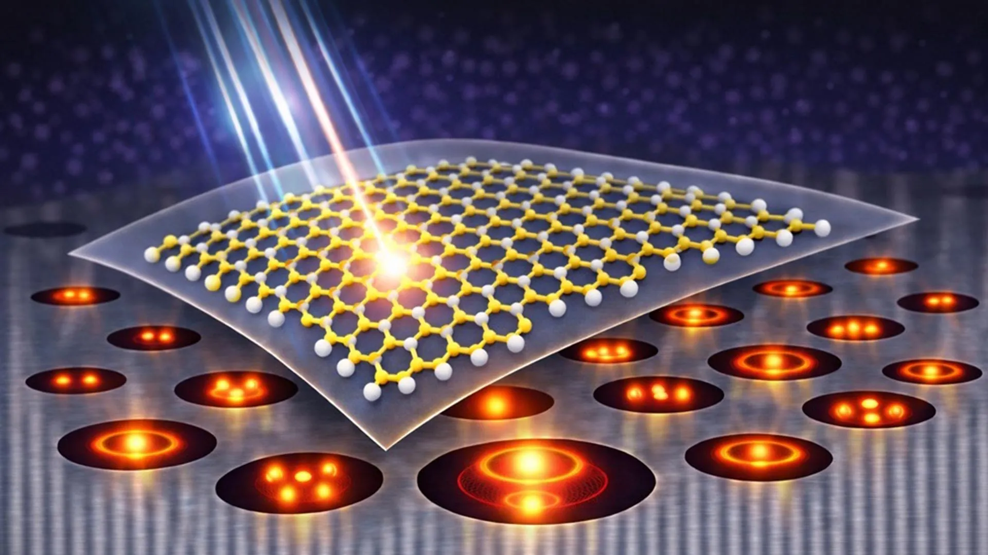
The field of nanophotonics has reached a significant milestone with the development of a novel architecture that dramatically enhances the optical properties of two-dimensional (2D) materials. Researchers have successfully demonstrated that by etching nanoscale air cavities—known as Mie voids—into a high-index substrate of bismuth telluride (Bi2Te3), they can amplify the light emission and nonlinear optical signals of a single layer of tungsten disulfide (WS2). This breakthrough, recently detailed in the journal Advanced Photonics, addresses one of the most persistent hurdles in the commercialization of 2D semiconductors: their inherent inefficiency in light-matter interaction due to their extreme thinness.
As the electronics industry approaches the physical limits of traditional silicon-based components, transition metal dichalcogenides (TMDCs) like tungsten disulfide have emerged as frontrunners for the next generation of photonic and optoelectronic devices. These materials, often only a single atom thick, possess unique quantum mechanical properties, including the ability to host stable excitons—bound states of electrons and holes—at room temperature. However, the same "atomically thin" nature that makes them ideal for miniaturization also limits their ability to absorb and emit light effectively. Without an engineered environment to concentrate electromagnetic fields, most light simply passes through the material without interacting.
The Evolution of Atomically Thin Semiconductors
The journey toward efficient 2D photonics began with the discovery of graphene, but it was the subsequent identification of TMDCs that provided the necessary direct bandgap for light emission. Tungsten disulfide, in its monolayer form, is particularly prized for its strong exciton resonance and its ability to facilitate nonlinear optical processes like second-harmonic generation (SHG), where two photons of the same frequency interact with the material to produce a single photon with twice the energy (and half the wavelength).
Despite these promising attributes, early attempts to integrate WS2 into functional devices were hampered by low quantum yields. Traditional methods to boost these signals involved placing the 2D layer atop dielectric nanoresonators, typically made of silicon or titanium dioxide. While these structures can trap light, they often confine the highest intensity of the electromagnetic field within the center of the solid resonator, away from the 2D material sitting on the surface. Furthermore, many high-index materials that could serve as resonators are also highly absorptive, which tends to dampen the resonance and reduce the overall efficiency of the system.
Engineering the Vacuum: The Mie Void Concept
The research team, led by international experts in nanophotonics, proposed a departure from traditional solid-state resonators. Instead of focusing on the material of the resonator itself, they focused on the "empty space" beneath the semiconductor. By utilizing Mie voids—subwavelength air cavities carved into a high-refractive-index medium—the researchers created an environment where light is reflected at the air-dielectric boundary and circulates within the void.
This "inverted" confinement strategy ensures that the maximum electromagnetic field intensity is located within the air cavity and at the top surface of the substrate. For a monolayer of WS2 placed over these voids, this means the material is positioned exactly where the optical field is strongest. The choice of bismuth telluride (Bi2Te3) as the host material was strategic. Although Bi2Te3 is a topological insulator known for its high absorption in the visible spectrum, its exceptionally high refractive index makes it an ideal candidate for supporting Mie resonances when configured as a void rather than a solid pillar.
Chronology of the Research and Experimental Design
The development of this heterostructure followed a rigorous multi-stage process involving theoretical modeling, precision fabrication, and advanced spectroscopic analysis.
- Computational Modeling: The team began by conducting extensive electromagnetic simulations to determine the optimal geometry for the voids. They targeted the "A-exciton" of WS2, the material’s primary emission feature. The simulations revealed that by adjusting the radius and depth of the voids to the scale of a few hundred nanometers, they could align the dipolar resonance of the cavity with the specific wavelength of the WS2 emission.
- Fabrication of Bi2Te3 Templates: Using mechanical exfoliation, the researchers prepared high-quality flakes of bismuth telluride. They then employed focused ion beam (FIB) milling to etch arrays of voids into the flakes. The voids were spaced at intervals large enough to prevent inter-cavity coupling, ensuring that each functioned as an isolated, independent resonator.
- Monolayer Integration: A continuous monolayer of WS2 was grown via chemical vapor deposition (CVD) or exfoliated and then transferred onto the patterned Bi2Te3 substrate. This resulted in a single sheet of WS2 covering a variety of environments: resonant voids, non-resonant voids of different sizes, and flat, unpatterned regions of the crystal.
- Optical Characterization: The team used micro-photoluminescence (PL) spectroscopy and reflection measurements to verify the resonance. By scanning the laser across the sample, they could compare the light output from the WS2 sitting over the voids against the output from the WS2 on the flat substrate.
Quantifying the Enhancement: Supporting Data
The experimental results provided definitive evidence of the efficacy of the Mie void approach. When the geometry of the cavity was tuned to match the A-exciton of the tungsten disulfide, the photoluminescence intensity increased by a factor of approximately 20 compared to non-resonant configurations.
Crucially, the researchers sought to determine whether this increase was simply due to the material absorbing more of the excitation laser. Their analysis, supported by wavelength-dependent experiments, confirmed that the enhancement was an "emission-side" effect. The Mie voids increase the local density of optical states (LDOS), a phenomenon known as the Purcell effect, which accelerates the rate of spontaneous emission. Additionally, the geometric shape of the void acts as a directional antenna, redirecting light that would normally be trapped in the substrate back toward the detector.
In the realm of nonlinear optics, the results were even more pronounced. Second-harmonic generation (SHG) is highly sensitive to local field intensity, as the signal scales quadratically with the input power. By shifting the cavity resonance to the near-infrared range to match the excitation laser, the researchers observed a 25-fold increase in the SHG signal.
Visualizing Light at the Nanoscale
One of the most significant secondary outcomes of the study was the ability to directly visualize optical modes. Traditional methods of observing how light behaves inside a nanoresonator often require complex near-field scanning optical microscopy (NSOM), which involves a physical probe moving nanometers above the surface.
In this study, the high-intensity hotspots created by the Mie voids were bright enough to be captured using standard far-field imaging of the SHG signal. As the researchers tuned the laser or moved across different cavity depths, they could see the light "moving" and localizing within the voids in real-time. This provides a new, non-invasive method for researchers to map electromagnetic fields in 2D heterostructures.
Expert Analysis and Implications
Industry analysts and members of the scientific community have reacted positively to the findings. Dr. Elena Rossi, a senior researcher in optoelectronics (not involved in the study), noted, "The transition from solid resonators to void-based confinement is a clever solution to the absorption losses that plague high-index materials. By turning the problem on its head—shaping the air instead of the matter—this team has opened a door for using a much wider array of materials in nanophotonic circuits."
The implications of this research extend into several high-tech sectors:
- Quantum Computing: Enhanced light-matter interaction is a prerequisite for creating reliable single-photon sources, which are the "bits" of quantum information.
- On-Chip Communications: Compact, efficient light sources that can be integrated into existing semiconductor manufacturing processes are essential for replacing slow copper wires with high-speed optical interconnects.
- Sensing and Diagnostics: The ability to amplify optical signals from surface-bound materials makes this platform ideal for biosensors capable of detecting single molecules or environmental pollutants.
- Nonlinear Frequency Conversion: Efficient SHG at the nanoscale could lead to ultra-compact devices that change the color of laser light for applications in imaging and spectroscopy.
A New Paradigm for Nanophotonics
The study published in Advanced Photonics represents more than just a technical improvement; it suggests a shift in how engineers approach the design of light-matter interfaces. By demonstrating that Bi2Te3—a material previously considered "too lossy" for high-performance photonics—can be transformed into a superior resonator through the use of Mie voids, the researchers have validated a versatile design principle.
This platform is inherently compatible with the "Lego-like" stacking of van der Waals materials, allowing for the creation of complex, multi-layered devices without the constraints of lattice matching required in traditional semiconductor growth. As the fabrication techniques for 2D materials continue to mature, the integration of Mie-void heterostructures may become a standard feature in the toolkit of nanophotonic engineering, providing the necessary "volume" for light to interact with the world of the infinitely thin.


Leave a Reply