
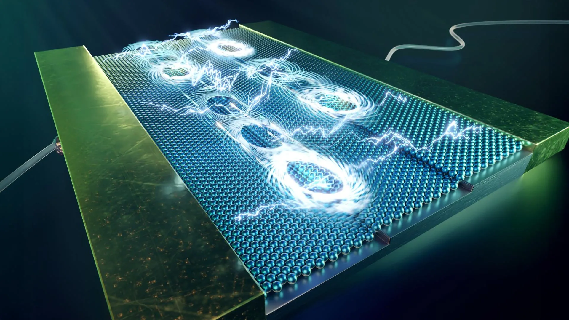
In a breakthrough that bridges the gap between quantum mechanics and nanoscale engineering, scientists in Japan have discovered that surface steps just one atom high can function as microscopic railroad tracks to direct the movement of quantum vortices. Conducted by researchers at the Research Center for Materials Nanoarchitectonics (MANA)—a premier institution operating under Japan’s National Institute for Materials Science (NIMS)—this study demonstrates that under specific physical conditions, these vortices move more than 1,000 times more easily along the atomic steps than across them. Furthermore, the research team established that this directional control can be dynamically adjusted simply by tuning external variables such as temperature or the strength of an applied magnetic field.
The findings, which were recently published in the peer-reviewed journal Physical Review B, shed light on a fundamental challenge in condensed matter physics: the precise control of quantum vortices in two-dimensional materials. By harnessing these atomic-scale structural features, engineers may soon be able to design superconducting electronic components that operate with radically lower energy consumption and drastically enhanced information processing capabilities.
The Fundamentals of Superconductivity and the Vortex Problem
To understand the significance of the MANA discovery, one must first examine the physics of superconductors. Discovered more than a century ago, superconductors are materials capable of conducting electrical current with absolute zero resistance when cooled below a critical material-specific temperature. In a normal conductor, moving electrons collide with atomic lattices, generating heat and wasting energy. In a superconductor, however, electrons form bound pairs known as Cooper pairs, which move collectively as a macroscopic quantum state, bypassing resistance altogether.
This zero-resistance property holds immense promise for global infrastructure, offering visions of lossless power transmission grids, ultra-fast maglev trains, and powerful magnets for medical imaging. More recently, superconductors have emerged as vital building blocks for quantum computing architectures, where fragile quantum bits, or qubits, require pristine electronic environments to maintain their states.
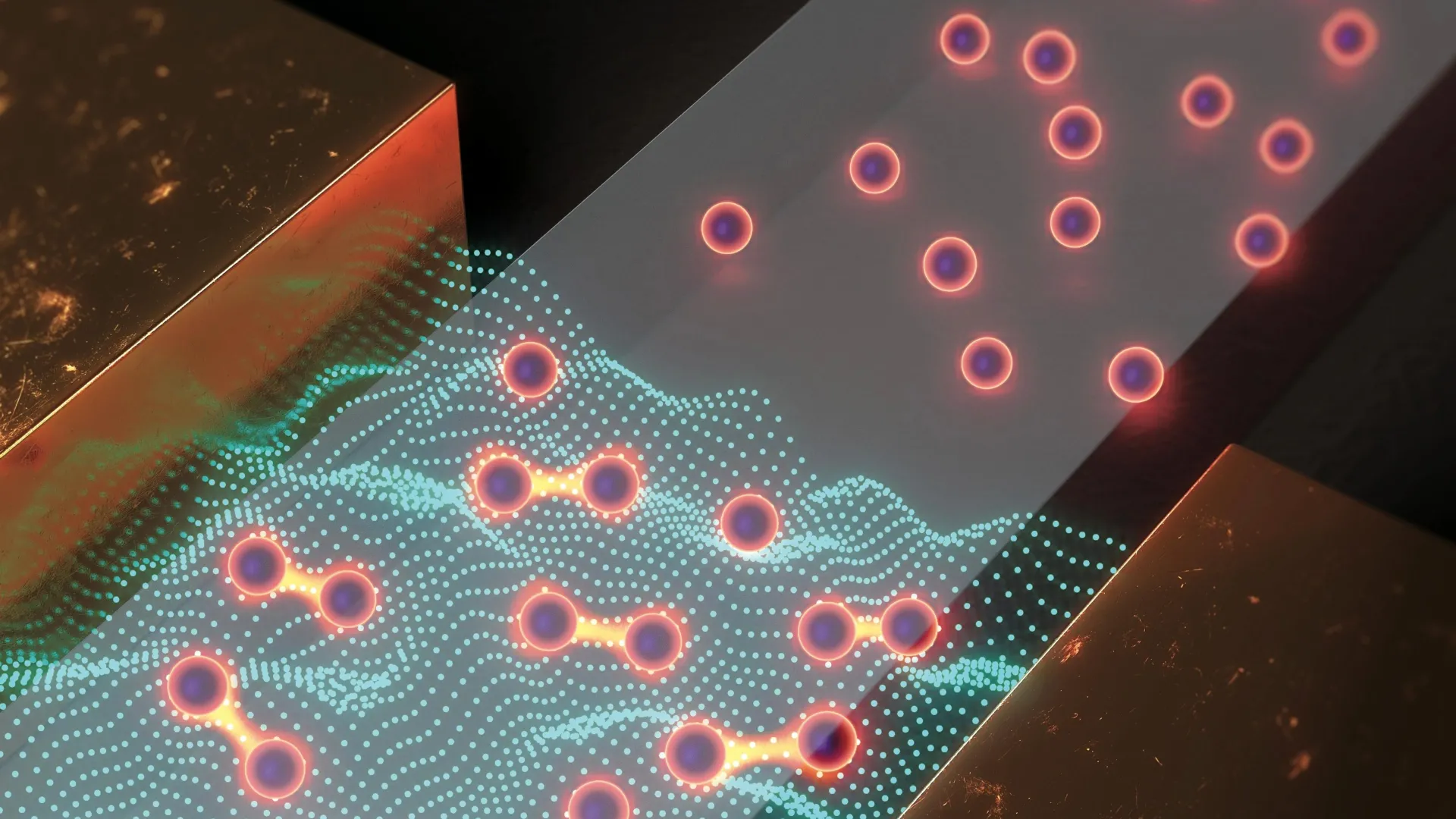
However, realizing these technologies is rarely straightforward. When certain types of superconductors—specifically Type-II superconductors—are exposed to an external magnetic field, the field does not simply blanket the material. Instead, it penetrates the superconductor in discrete, quantized filaments known as flux lines or quantum vortices. Each vortex forms a tiny region where the superconducting state is locally suppressed, surrounded by a persistent circulating vortex of electrical supercurrent.
The central problem for device engineers is that these vortices are rarely static. When an electrical transport current passes through a superconductor, it exerts a Lorentz force on the vortices, causing them to move. As these vortices travel across the material, their motion induces a viscous drag and generates an electric field, which translates directly back into electrical resistance. This resistance destroys the ideal zero-loss state of the superconductor and generates unwanted thermal energy, degrading the performance of sensitive electronic devices.
For decades, controlling the trajectory of these vortices in bulk materials has been a major objective for physicists, typically achieved by introducing artificial pinning centers such as nanoscale holes, chemical impurities, or defects. However, achieving this level of control in ultrathin, two-dimensional superconductors—where quantum fluctuations are amplified and space is constrained to atomic dimensions—has remained an elusive goal.
Chronology of the Research and Experimental Methodology
The path to this discovery began with a focused initiative at MANA to investigate the fundamental electrodynamic properties of atomically thin layers. Led by senior researcher Takashi Uchihashi, the research team sought to determine whether natural, periodic topographic features on a substrate could be leveraged to corral quantum vortices, rather than treating surface imperfections as manufacturing flaws to be eliminated.
To investigate this hypothesis, the Uchihashi-led team fabricated an ultrathin superconducting sample characterized by a surface topography featuring a series of regularly spaced, parallel atomic steps—ridges and terraces measuring only a single atom in height.
The investigation relied heavily on advanced surface-imaging technology. Utilizing ultra-high-vacuum scanning tunneling microscopy (STM), a sophisticated imaging technique capable of mapping surfaces with sub-nanometer resolution down to the individual atom, the researchers mapped the atomic topography of the superconductor. Through STM imaging, the team confirmed that the atomic steps ran in parallel arrays across the material and successfully observed individual quantum vortices localized along these specific topographical boundaries.
Following the imaging phase, the team subjected the sample to rigorous electrical transport experiments. They employed a four-terminal resistance measurement configuration—a standard metrological technique used to eliminate lead and contact resistance—to precisely measure electrical conductivity and resistance along and across the atomic steps under varying physical environments.
Quantifying the Atomic Railway Effect: Supporting Data
The quantitative results of the four-terminal resistance measurements revealed an extraordinary anisotropy in vortex mobility. When the superconducting sample was exposed to intermediate magnetic fields, vortices traveled more than 1,000 times more easily along the direction of the atomic steps than they did perpendicularly across them.
This profound disparity confirmed the hypothesis that atomic steps act as efficient, unidirectional pathways—effectively functioning as quantum-scale railway tracks. The step edges create local variations in the superconducting order parameter, forming an energetic landscape where vortices find it energetically favorable to remain confined to the trough of the step rather than climbing over the atomic ridge.
Further data analysis within specific magnetic field regimes revealed additional nuance. When the applied magnetic field was maintained within a window of approximately 0.10 to 0.20 tesla (T), the researchers observed a phenomenon designated as one-dimensional pinning-free vortex flow. In this operational regime, vortices could travel smoothly and continuously along the atomic steps without experiencing the typical trapping or scattering effects caused by random material defects or impurities. This smooth, unobstructed flow is a critical requirement for maintaining low dissipation in superconducting circuits.
At the lowest temperature thresholds evaluated in the study, the research team documented the manifestation of quantum tunneling governing vortex dynamics. Rather than relying on classical thermal activation to surmount energy barriers, the quantum vortices demonstrated the ability to tunnel directly through these barriers, a demonstration of macroscopic quantum phenomena operating at experimental scales.
Official Responses and Scientific Interpretations
In statements accompanying the publication of their findings, members of the MANA research group emphasized the versatility and control enabled by their approach.
"Our study shows that atomic-scale steps can act as effective rails that guide superconducting vortices, and that this guiding effect can be tuned simply by changing the temperature or magnetic field," stated Dr. Takashi Uchihashi, lead investigator of the project.
Independent condensed matter physicists and materials scientists not directly involved in the study have echoed these sentiments, noting that the ability to manipulate vortex trajectories without introducing disruptive chemical dopants represents a significant methodological advancement. By utilizing the intrinsic topology of the crystal lattice or the substrate interface, manufacturers can avoid introducing random disorder that often degrades the overall electronic quality of superconducting films.
While institutional representatives from Japan’s National Institute for Materials Science have not yet announced commercial commercialization timelines, they have highlighted the foundational nature of the discovery. The MANA center, known globally for its pioneering work in nanoarchitectonics—the arrangement of atoms and molecules into functional macroscopic structures—views this work as a prime example of how structural design at the atomic scale can yield macroscopic control over quantum states.
Broader Impacts and Technological Implications
The implications of this discovery extend across several domains of advanced technology, offering a conceptual blueprint for the next generation of superconducting electronics.
Chief among these potential applications is the development of ultra-low-power electronic devices. Modern semiconductor manufacturing faces fundamental thermodynamic limits related to heat dissipation and power consumption, driving interest in alternative paradigms such as superconductivity-based logic and memory circuits. By learning to direct vortex motion along designated, lossless channels, engineers can design circuits where energy loss due to vortex migration is minimized or completely engineered away.
Furthermore, these findings may impact the development of superconducting quantum computers. Qubits based on Josephson junctions and superconducting circuits are exceptionally sensitive to magnetic noise and stray vortex motion. Uncontrolled vortex migration can introduce magnetic flux noise, leading to decoherence and operational errors in quantum processors. By utilizing atomic-scale guiding tracks, quantum hardware engineers could systematically route stray vortices away from sensitive active regions, thereby improving the coherence times and overall fidelity of superconducting quantum processors.
Beyond computing, the ability to control vortex dynamics and associated thermal transport opens pathways for advanced cryogenic sensors, high-precision magnetometry, and lossless power management systems. As cooling technologies become more compact and reliable, the integration of atom-scale topographic engineering into device fabrication could transition from a laboratory curiosity into a standard manufacturing protocol.
Future Outlook and Ongoing Research
As the scientific community digests the findings published in Physical Review B, the MANA research team and collaborating laboratories are already planning subsequent phases of investigation. Future studies are expected to focus on scaling these atomic guiding tracks across larger surface areas, testing alternative superconductor-substrate material combinations, and integrating these guided vortex structures into functional prototype devices.
While considerable engineering challenges remain before these concepts transition into commercial hardware, the discovery in Japan underscores the profound potential of materials nanoarchitectonics. By learning to read and write the rules of quantum behavior using features just one atom high, researchers are steadily dismantling the barriers that have long separated quantum mechanics from practical, everyday engineering.