
The field of nanophotonics has reached a pivotal juncture where the demand for ultra-compact, high-efficiency light sources is driving researchers to explore the limits of two-dimensional (2D) materials. A landmark study recently published in the journal Advanced Photonics has unveiled a sophisticated method for overcoming the inherent limitations of atomically thin semiconductors, specifically tungsten disulfide (WS₂). By engineering the photonic environment beneath these materials using high-index dielectric "Mie voids," researchers have demonstrated a significant amplification of both linear and nonlinear optical responses. This breakthrough provides a scalable and robust platform for next-generation optoelectronic devices, quantum sensing, and on-chip photonic circuits, marking a departure from traditional light-trapping techniques that often struggle with the extreme thinness of van der Waals materials.
The Evolution and Limitations of 2D Semiconductors
Over the past decade, transition metal dichalcogenides (TMDCs) like WS₂ have emerged as the frontrunners for future electronic and photonic applications. When reduced to a single layer of atoms, these materials undergo a transition from an indirect bandgap to a direct bandgap, allowing them to interact strongly with light. This interaction is primarily mediated by excitons—tightly bound pairs of electrons and holes that possess high oscillator strength. Despite these remarkable properties, the physical reality of being only 0.7 nanometers thick presents a formidable challenge: the interaction volume between the material and incident light is exceedingly small.
In a typical setting, a monolayer of WS₂ absorbs only a fraction of incoming photons, and its light emission, while present, is often too weak for practical applications in integrated systems. To combat this, scientists have historically turned to photonic crystals, plasmonic nanoparticles, or dielectric resonators to "squeeze" light into the material. However, traditional designs often trap the maximum intensity of the light field inside the solid bulk of the resonator (such as a silicon nanopillar), leaving the 2D material, which sits on the surface, exposed only to the weaker evanescent tails of the optical mode. Furthermore, many high-index materials that could serve as resonators suffer from parasitic absorption, which dampens the resonance and limits the overall efficiency of the system.
A Paradigm Shift: The Architecture of Mie Voids
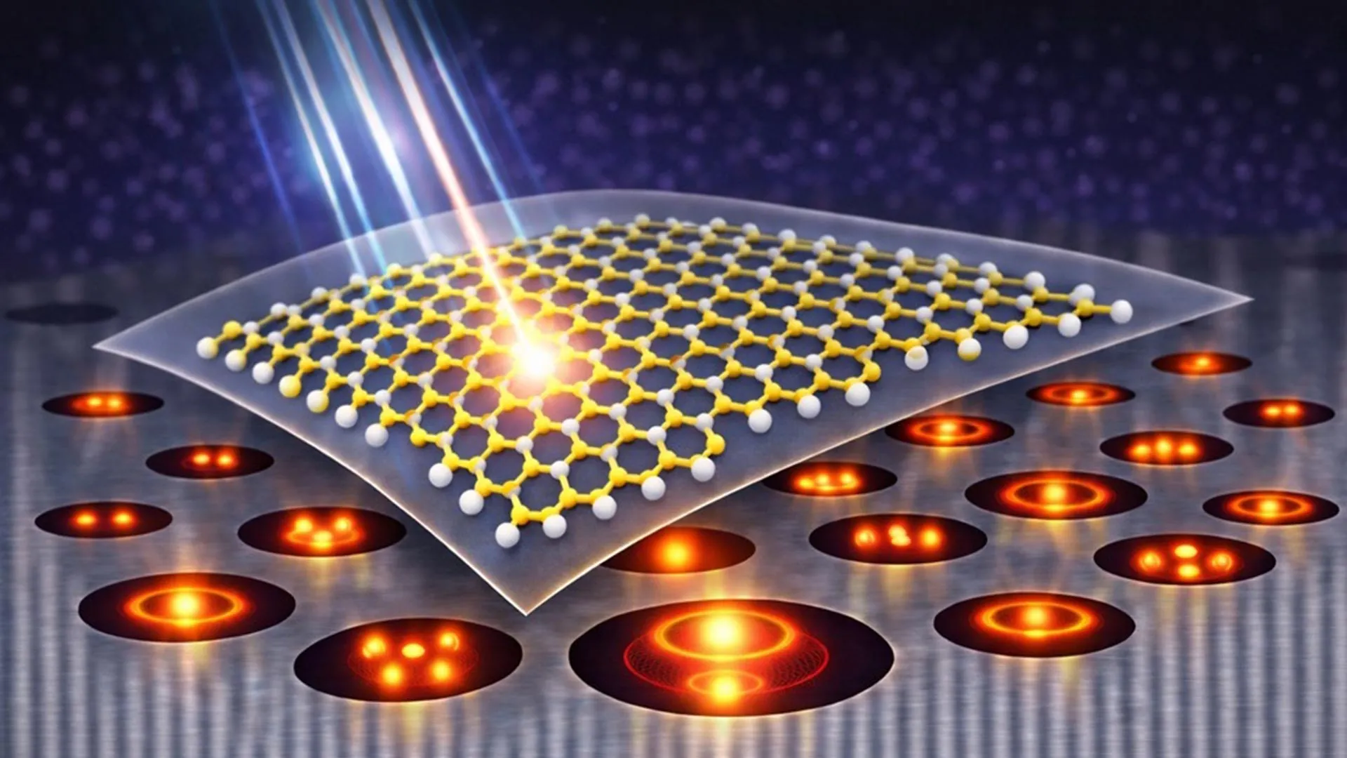
The research team behind the Advanced Photonics study proposed a radical inversion of the standard resonator design. Instead of using solid nanostructures, they utilized "Mie voids"—subwavelength air cavities etched into a high-index substrate of bismuth telluride (Bi₂Te₃). Bismuth telluride is a material known for its high refractive index, which is essential for strong light confinement, yet it is also highly absorptive in the visible spectrum. In a conventional solid resonator, this absorption would be a deal-breaker. However, by using the material as a "mold" for an air cavity, the researchers were able to confine the light within the empty space of the void.
This "inverted" confinement strategy ensures that the peak of the electromagnetic field is located within the air region and at the top interface of the cavity. Because the WS₂ monolayer is transferred directly over these voids, it sits precisely where the light field is most intense. This alignment maximizes the light-matter interaction without the energy losses typically associated with absorption in the resonator material itself. The Mie voids function as high-quality optical resonators that can be precisely tuned by varying their geometric parameters, such as radius and depth.
Chronology of Development and Experimental Design
The development of these Mie-void heterostructures followed a rigorous multi-stage process, beginning with theoretical modeling and concluding with advanced optical characterization.
- Electromagnetic Simulation (Phase I): The researchers began by using finite-difference time-domain (FDTD) simulations to predict the behavior of light within Bi₂Te₃ cavities. They specifically sought to design a dipolar resonance that would overlap with the A-exciton emission of WS₂, which typically occurs around 620–630 nm. The simulations revealed that by adjusting the depth of the cavity, they could control the vertical position of the optical mode, ensuring it "leaked" slightly above the surface to interact with the 2D layer.
- Substrate Preparation and Milling (Phase II): The team utilized thick flakes of Bi₂Te₃, obtained through mechanical exfoliation. Using Focused Ion Beam (FIB) milling, they carved arrays of nanovoids into the flakes. To ensure that each cavity acted as an isolated resonator, the voids were spaced several micrometers apart, preventing optical crosstalk and allowing for the study of individual cavity dynamics.
- Monolayer Integration (Phase III): A continuous monolayer of WS₂, grown via chemical vapor deposition (CVD) or exfoliated, was transferred onto the patterned Bi₂Te₃ substrate using a dry-transfer technique. This created a heterostructure where the WS₂ film acted as a "drumhead" covering the various air cavities.
- Characterization (Phase IV): The final stage involved comprehensive optical testing, including micro-reflectance spectroscopy to confirm the resonance positions, photoluminescence (PL) mapping to measure light emission enhancement, and second-harmonic generation (SHG) microscopy to evaluate nonlinear performance.
Empirical Data: Quantifying the Enhancement
The results of the experiments provided clear evidence of the effectiveness of the Mie-void approach. When the geometry of the cavity was optimized to match the A-exciton of the WS₂, the photoluminescence intensity increased by a factor of approximately 20 compared to non-resonant regions of the same sample. This enhancement was attributed to two primary factors: an increase in the local density of optical states (LDOS), known as the Purcell effect, and an improved extraction efficiency, which helps the emitted light escape the substrate and reach the detector.
Crucially, the researchers verified that this boost was not merely a result of increased absorption of the excitation laser. By testing various pump wavelengths, they found that the emission enhancement remained tied to the cavity’s resonance at the emission wavelength, rather than the excitation wavelength.
In the realm of nonlinear optics, the results were even more pronounced. Nonlinear effects like second-harmonic generation (SHG)—where two photons of a certain frequency are converted into one photon of double the frequency—are extremely sensitive to local field intensity. By tuning the Mie voids to resonate at the near-infrared excitation wavelength (approximately 1240 nm), the researchers observed a 25-fold increase in the SHG signal. This demonstrated that the Mie-void platform is versatile enough to enhance different optical processes simply by scaling the cavity dimensions.
Direct Visualization of Optical Modes
One of the most compelling aspects of this research is the ability to directly visualize the behavior of light at the nanoscale. Because the SHG signal is so closely tied to the local field distribution, the researchers were able to use far-field SHG imaging to map the optical modes within the cavities.
The images revealed distinct "hotspots" of light located directly above the centers of the resonant voids. As the excitation wavelength was tuned or the cavity depth was varied, the researchers could watch these hotspots evolve in real-time. This provided a "real-space" look at Mie resonances that is typically only possible through complex near-field scanning optical microscopy (NSOM). This capability is significant for the broader scientific community, as it offers a simpler way to verify and study the internal physics of nanophotonic structures.
Analysis of Implications and Industry Potential
The success of the Bi₂Te₃-WS₂ Mie-void heterostructure has several far-reaching implications for the photonics industry and fundamental physics.
Overcoming Material Constraints: Historically, nanophotonics has been limited by the "transparency window" of materials like silicon or gallium phosphide. The Mie-void design proves that even highly absorptive, "lossy" materials can be used to create high-performance resonators, provided the light is confined in the air fraction of the structure. This opens up a vast library of new materials, including topological insulators and narrow-bandgap semiconductors, for use in photonic design.
On-Chip Integration: The compact nature of these individual resonators makes them ideal for integration into dense photonic chips. Unlike metasurfaces, which require large periodic arrays to function, a single Mie void can provide significant enhancement. This could lead to the development of ultra-small, low-power light sources for optical computing and data transmission.
Sensing and Quantum Optics: The enhanced field at the surface of the void is perfectly positioned for sensing applications. Molecules placed on the WS₂ layer would experience the same field enhancement, potentially allowing for the detection of single molecules through surface-enhanced Raman scattering (SERS) or enhanced fluorescence. Furthermore, the ability to control the emission of 2D excitons is a critical step toward creating reliable single-photon sources for quantum communication.
Conclusion and Future Outlook
While the study focused on the WS₂ and Bi₂Te₃ system, the researchers emphasize that this is a generalizable platform. The same principles could be applied to other 2D materials, such as molybdenum disulfide (MoS₂) or even graphene, and other high-index substrates.
Experts in the field suggest that the next step will be to move toward "programmable" photonic devices. By integrating these heterostructures with electrical gating or thermal tuning, it may be possible to switch the resonance on and off or shift its wavelength dynamically. This would pave the way for high-speed optical modulators and tunable filters that are only atoms thick.
The findings presented in Advanced Photonics underscore a fundamental shift in nanophotonic strategy: the realization that the empty space surrounding a material can be just as influential as the material itself. By carefully shaping the "nothingness" of a nanovoid, scientists have unlocked a new level of performance from the world’s thinnest semiconductors, bringing us one step closer to a future defined by light-based technology.


Leave a Reply