

The field of photonics has reached a significant milestone as researchers from the XPANCEO Emerging Technologies Research Center, in a high-profile collaboration with Nobel Laureate Professor Konstantin Novoselov, have announced the discovery of unprecedented optical properties in crystalline arsenic trisulfide (As2S3). This material, a member of the van der Waals semiconductor family, demonstrates a transformative response to light that allows for the permanent, high-precision alteration of its internal structure at the nanoscale. By utilizing simple continuous-wave (CW) light rather than the prohibitively expensive and complex femtosecond laser systems or traditional cleanroom lithography, the team has unlocked a more accessible pathway for the fabrication of next-generation optical devices. This discovery marks a pivotal shift in how scientists approach the manipulation of light, moving away from labor-intensive mechanical manufacturing toward a more fluid, light-driven methodology.
The Mechanics of Photorefractivity in Van Der Waals Semiconductors
At the heart of this scientific advancement lies the principle of the refractive index, a fundamental metric in optics that dictates how light propagates through a medium. The refractive index determines both the speed of light within the material and the degree to which light rays are bent upon entry. In the pursuit of miniaturizing optical components, materials with high refractive indices are prized for their ability to confine light within extremely small volumes, which is essential for the development of compact sensors, waveguides, and integrated photonic circuits.
The phenomenon known as photorefractivity occurs when a material’s refractive index changes in response to light exposure. While this effect has been documented in various substances, the magnitude of the change observed in crystalline As2S3 is what has captured the attention of the global scientific community. The research team reported a refractive index shift of up to Δn ≈ 0.3. To put this figure into perspective, this change is significantly larger than those observed in industry-standard photorefractive materials such as Lithium Niobate (LiNbO3) or Barium Titanate (BaTiO3), which are currently the backbone of telecommunications and laser modulation technologies.
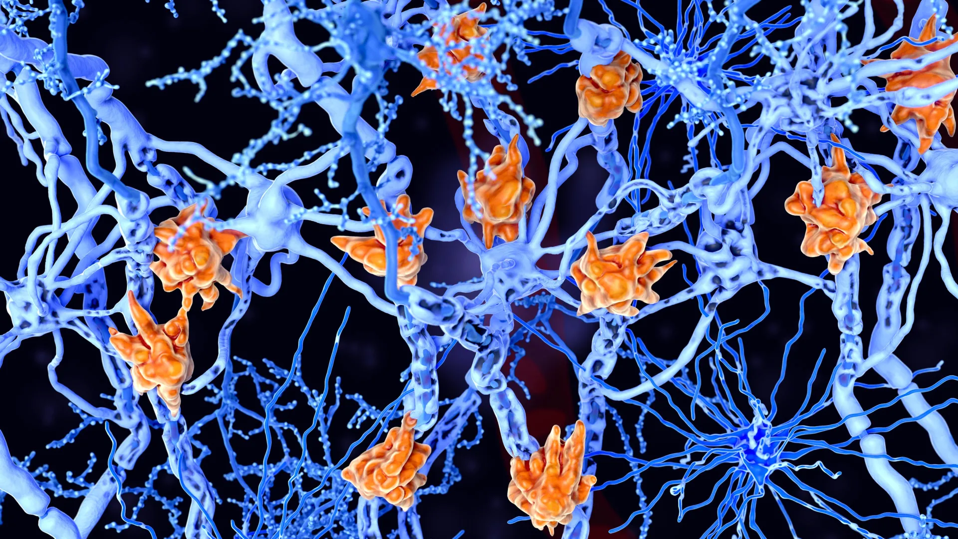
What makes As2S3 particularly unique is its status as a van der Waals (vdW) crystal. These materials are characterized by strong covalent bonds within individual atomic layers, which are held together by weak van der Waals forces. This layered structure allows for exceptional control over the material’s electronic and optical properties. In the case of As2S3, the crystalline lattice responds to ultraviolet (UV) light by undergoing a permanent structural reorganization, effectively "freezing" the light-induced changes into the material without the need for subsequent chemical processing.
Chronology of the Discovery and Research Development
The journey toward this discovery is rooted in the broader evolution of two-dimensional (2D) materials research, a field ignited by the isolation of graphene in 2004 by Professor Konstantin Novoselov and Professor Andre Geim. Since then, the focus of the scientific community has expanded from graphene to a wider array of vdW crystals, including transition metal dichalcogenides and chalcogenide glasses.
The specific investigation into As2S3 began several years ago as researchers sought materials that could bridge the gap between traditional semiconductors and flexible, transparent electronics. While amorphous arsenic trisulfide (glassy As2S3) has long been used in infrared optics, its crystalline counterpart remained relatively under-explored regarding its photorefractive potential.
The XPANCEO-led project underwent several rigorous phases:
- Material Synthesis: The team perfected the growth of high-purity crystalline As2S3 flakes, ensuring a uniform lattice structure capable of supporting stable optical changes.
- Optical Characterization: Using spectroscopic methods, the researchers mapped the material’s response to various wavelengths of light, discovering that low-intensity CW light was sufficient to trigger a massive refractive index shift.
- Nanoscale Patterning: The team moved to practical demonstrations, testing the limits of how small a pattern could be "written" into the crystal.
- Structural Analysis: Post-exposure analysis confirmed that the changes were not merely electronic but involved a physical expansion of the lattice, providing a dual mechanism for optical control.
Experimental Data: Pushing the Limits of Resolution
To demonstrate the precision of their light-driven fabrication technique, the researchers performed a series of high-resolution experiments. Using a standard, low-power laser, they successfully "printed" a monochrome portrait of Albert Einstein onto a thin flake of As2S3. The resolution achieved was staggering: the points making up the image were spaced just 700 nanometers apart.
Further optimization of the laser-writing process revealed that the material could support even finer details. The researchers achieved a resolution equivalent to 50,000 dots per inch (DPI), with features spaced at approximately 500 nanometers. This resolution is near the diffraction limit of visible light, meaning the material can store information or guide light at the smallest scales physically possible for such optical systems.
A secondary but equally significant finding was the physical response of the material. Beyond the change in refractive index, the As2S3 crystal expanded by up to 5% in volume in the areas exposed to light. This light-induced swelling allows for the direct creation of three-dimensional topographical features on the surface of the material. Researchers can essentially "grow" microlenses and diffraction gratings directly onto the crystal surface simply by shining light on it. This eliminates the need for etching or material deposition, two of the most expensive and time-consuming steps in traditional semiconductor manufacturing.
Official Responses and Industry Significance
The implications of this research are far-reaching, particularly for the burgeoning field of wearable technology and human-machine interfaces. Valentyn Volkov, the Founder and Chief Technology Officer at the XPANCEO Emerging Technologies Research Center, emphasized the foundational nature of the discovery.
"The discovery of new functional materials, particularly within the unique family of van der Waals crystals, is the fundamental engine for moving the entire field of photonics forward," Volkov stated. "Developing sophisticated optical devices, such as advanced smart contact lenses, is a deeply complex challenge that requires a solid foundation in fundamental materials science. In these systems, the material itself is the key component that determines what is physically possible. By identifying natural crystals with this level of sensitivity, we are effectively providing the essential building blocks for a new generation of technology that is driven entirely by light rather than electricity."
The involvement of Professor Konstantin Novoselov adds a layer of academic validation that is expected to accelerate the adoption of vdW materials in commercial R&D. Industry analysts suggest that the ability to fabricate optical components without a cleanroom could democratize the production of high-end sensors and telecommunications hardware, allowing smaller firms and research labs to innovate without the multi-million dollar overhead of traditional fabrication facilities.
Broader Impact: From Anti-Counterfeiting to Smart Contact Lenses
The practical applications of this "optical writing" technique are diverse. One of the most immediate uses is in the field of security and authentication. Because the light-induced patterns in As2S3 are embedded within the material and possess a unique "optical fingerprint" based on the refractive index shift, they are nearly impossible to forge. This could lead to a new generation of anti-counterfeiting labels for high-value goods, pharmaceutical packaging, and sensitive documents.
In the realm of telecommunications, the ability to create high-contrast waveguides with a Δn of 0.3 means that optical signals can be routed through much tighter turns and more compact circuits than currently possible. This could lead to a significant reduction in the size of the optical transceivers that power the internet.
However, the most ambitious application lies in the development of smart contact lenses and augmented reality (AR) glasses. Current AR technology often struggles with a narrow field of view and bulky hardware, largely due to the limitations of the optical combiners used to project images into the eye. The 5% expansion property of As2S3, combined with its high refractive index, makes it an ideal candidate for creating wide field-of-view waveguides that are thin enough to be integrated into a standard contact lens.
Analysis of Future Implications
As the world moves toward an era of "ambient computing," where technology is seamlessly integrated into our physical environment, the reliance on traditional silicon-based electronics is being challenged. Light-driven materials like As2S3 offer a glimpse into a future where "photonic logic" replaces or augments electronic processing.
The efficiency of CW light for patterning suggests a future where manufacturing is not only cheaper but also more sustainable. Traditional lithography involves harsh chemicals, high vacuum environments, and significant energy consumption. In contrast, the XPANCEO method points toward a "green nanophotonics" where light itself is the primary tool of construction.
The success of this collaboration between a commercial research center and a Nobel-winning academic highlights a growing trend in the tech industry: the convergence of fundamental physics and rapid-prototyping engineering. As researchers continue to explore the vast library of van der Waals materials, it is likely that As2S3 is only the first of many crystals to reveal "super-properties" that will redefine the boundaries of what is possible in the age of light.


Leave a Reply