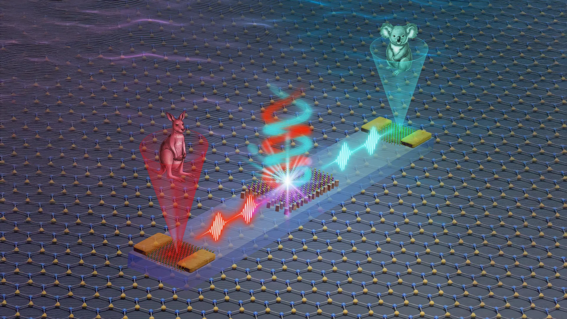
The quest to transition from bulky, frame-heavy wearable electronics to seamless, nearly invisible technologies has reached a significant milestone following a collaborative research effort between international academic institutions and private industry. A research team comprising scientists from XPANCEO, the National University of Singapore (NUS), and the University of Chemistry and Technology, Prague, has successfully mapped the complex optical properties of molybdenum oxychloride (MoOCl₂). This layered crystal, once a niche subject of study in solid-state physics, is now being hailed as a foundational material for the next generation of augmented reality (AR) glasses and smart contact lenses. By demonstrating the strongest light-bending effect ever recorded in a natural material, the study provides the essential data required to replace traditional, centimeter-scale glass lenses with nanometer-scale crystalline films.
The Shift Toward Atomic-Scale Nanophotonics
For decades, the field of optics has been defined by the physical limitations of glass and plastic. Traditional lenses rely on their geometric curvature to refract light, a process that inherently requires a certain volume of material to function. As the consumer electronics industry pushes toward "invisible" wearables—devices that integrate directly into the user’s field of vision without the weight of traditional hardware—these physical limitations have become the primary bottleneck.
The research published in Nano Letters addresses this challenge by shifting the focus from the shape of a lens to the internal atomic structure of the material itself. Molybdenum oxychloride belongs to a class of van der Waals materials, which are composed of layers held together by weak intermolecular forces. This structural arrangement allows researchers to manipulate light at the sub-wavelength scale, effectively doing with a few atomic layers what previously required thick glass components.
A Chronology of Discovery: From Theory to Measurement
The journey to understanding MoOCl₂ has evolved through several critical stages over the last few years. While the material has been known to physicists for its unique electronic properties, its potential for visible-light optics is a relatively recent revelation.
In early 2024, studies published in high-impact journals such as Science and Nature Communications began to highlight the material’s ability to support hyperbolic plasmon polaritons—tightly confined electromagnetic waves that travel along the surface of the crystal. These initial findings proved that MoOCl₂ could guide light in highly directional ways, far exceeding the capabilities of graphene or other well-known 2D materials.
However, a significant gap remained between observing these phenomena and being able to use them in engineering. Until now, the full "dielectric tensor"—the mathematical map of how a material interacts with electric fields in all three dimensions—had not been experimentally determined for MoOCl₂. The latest research from XPANCEO and its partners fills this void, providing the precise numerical values that optical engineers require to design functional devices. This transition from "observation" to "measurement" marks the official entry of MoOCl₂ into the toolkit of practical optoelectronics.
The Optical Chameleon: Anisotropy and Birefringence
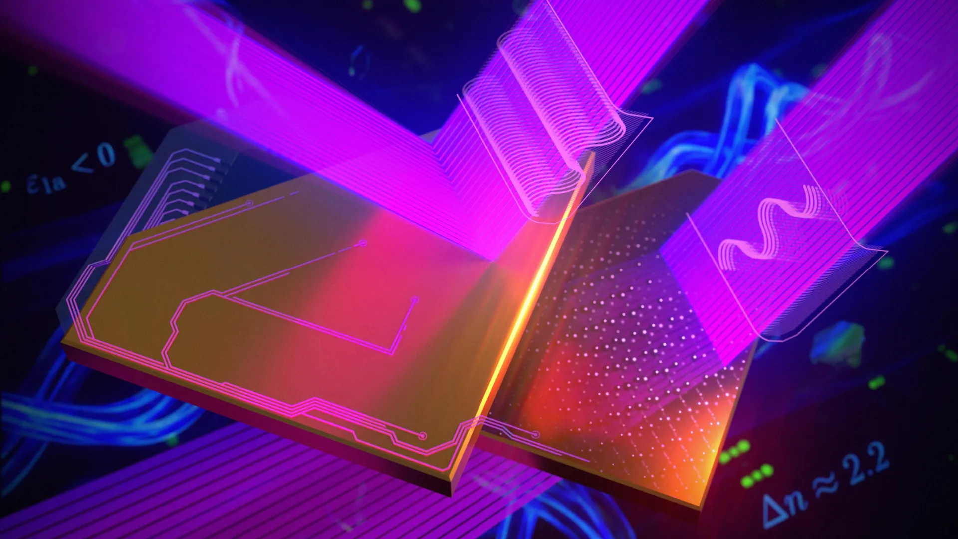
The core of the material’s appeal lies in its extreme optical anisotropy. In most common materials, such as water or standard glass, light behaves the same way regardless of the direction in which it travels. MoOCl₂ breaks this symmetry. The research team describes the crystal as an "optical chameleon" because its physical appearance and interaction with light change based on its orientation.
When the crystal is oriented along one axis, it behaves like a metal, reflecting light with high efficiency. When rotated 90 degrees, it transforms into a dielectric material, becoming as transparent as glass. This duality is a direct result of the material’s internal structure, which consists of one-dimensional chains of molybdenum atoms. Electrons move with relative ease along these chains (metallic behavior) but encounter high resistance when moving across them (insulator behavior).
This internal lopsidedness results in an in-plane birefringence value of approximately 2.2. To put this in perspective, calcite, a material traditionally used in optics for its light-splitting properties, has a birefringence of roughly 0.17. The fact that MoOCl₂ exhibits a value more than ten times higher means it can manipulate the polarization and direction of light within a thickness thousands of times thinner than a human hair.
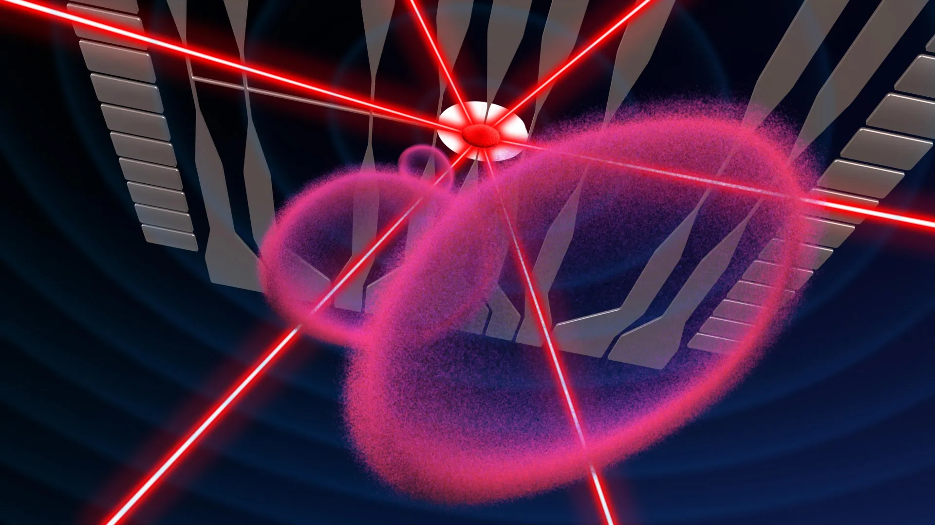
The Green Light Breakthrough: Epsilon-Near-Zero (ENZ) Phenomena
One of the most technically significant findings of the study is the identification of an "epsilon-near-zero" (ENZ) point at the 512-nanometer wavelength. This specific wavelength corresponds to green light, which is situated at the center of the visible spectrum and is the color to which the human eye is most sensitive.
At the ENZ point, the material’s permittivity (its ability to store electrical energy) approaches zero. This creates a unique physical environment where the phase velocity of light becomes nearly infinite, effectively "slowing" the light’s energy while the electric field inside the crystal is dramatically amplified.
In practical terms, this ENZ behavior allows for "sub-diffractional" optics. Normally, light cannot be squeezed into a space smaller than half of its wavelength. However, by using the ENZ properties of MoOCl₂, researchers can concentrate electromagnetic energy into incredibly small volumes. This is a critical requirement for creating integrated photonic chips, where light must be routed and processed within the microscopic confines of a computer processor.
Industry Implications: Beyond the Laboratory
The mapping of MoOCl₂ has immediate implications for several high-growth sectors in the technology industry.
1. Augmented Reality and Smart Contact Lenses
Current AR glasses, such as those produced by Meta or Microsoft, still require relatively bulky waveguides to project digital images onto the user’s eyes. The use of MoOCl₂ could allow these waveguides to be miniaturized to the point where they are integrated into a standard contact lens. The material’s ability to control light polarization and direction with high efficiency ensures that the projected images remain sharp and vibrant without the need for heavy power sources.
2. High-Speed Telecommunications and Photonic Computing
As traditional silicon-based electronics approach their physical limits, the industry is looking toward photonics—using light instead of electrons to process data. The strong light-matter interactions enabled by MoOCl₂’s ENZ point could lead to the development of optical switches and modulators that are faster and more energy-efficient than current components.
3. Advanced Sensing and Microscopy
The ability to concentrate light into sub-wavelength spaces has profound implications for biological and chemical sensing. Sensors utilizing MoOCl₂ could potentially detect single molecules or track chemical reactions in real-time with unprecedented sensitivity, benefiting both medical diagnostics and environmental monitoring.
Official Perspectives and Analysis
Dr. Valentyn Volkov, the founder and CTO of XPANCEO and the corresponding author of the study, emphasized that this research provides the necessary foundation for a new era of engineering. "Observing a phenomenon is the first step, but engineering requires precise numbers," Volkov stated. He noted that by rigorously measuring the complete dielectric tensor, the team has provided the "experimental foundation" needed to design around this material with confidence.
Industry analysts suggest that the involvement of a private entity like XPANCEO alongside major universities indicates a shortening timeline between fundamental material science and commercial application. While graphene took decades to move from the lab to specialized industrial use, the infrastructure for 2D material fabrication has matured significantly, potentially allowing MoOCl₂-based devices to reach the market within the next decade.
Challenges and the Path Forward
Despite the excitement surrounding these findings, several hurdles remain before MoOCl₂ becomes a household name. Layered crystals are notoriously difficult to manufacture at scale; while "exfoliating" small flakes in a lab is common, creating large-area, high-quality films for mass-produced electronics requires advanced chemical vapor deposition (CVD) techniques.
Furthermore, the environmental stability of oxychlorides must be thoroughly vetted. Many 2D materials are sensitive to moisture and oxygen, which could degrade their optical performance over time. Future research will likely focus on "encapsulation" techniques—sandwiching the MoOCl₂ between protective layers to ensure longevity in consumer devices.
The mapping of molybdenum oxychloride represents a pivotal shift in how we approach the hardware of the future. By moving away from the "bulk" optics of the 20th century and embracing the "atomic" optics of the 21st, researchers have opened a door to a world where technology is no longer something we carry or wear, but something that is seamlessly integrated into our very perception of reality. The green light at 512 nm may very well be the "go" signal for a new generation of invisible technology.