Researchers at the University of Cambridge and Swansea University have unveiled a transformative approach to terahertz (THz) detection, successfully integrating quantum physics with engineered metasurfaces to overcome long-standing barriers in the "terahertz gap." The study, recently published in the journal Advanced Photonics, details the development of a compact, high-sensitivity detector that utilizes a two-dimensional electron gas (2DEG) and a specialized "brickwork" metasurface. By concentrating electromagnetic energy into nanometric regions, the team achieved a twenty-fold increase in external quantum efficiency compared to previous iterations of similar quantum detectors. This advancement marks a critical step toward the miniaturization and commercialization of terahertz technologies, which have historically been limited by the need for bulky cryogenic cooling and inefficient signal conversion.
The Terahertz Gap and the Evolution of Detection Technology
The terahertz region of the electromagnetic spectrum, typically defined as the frequency range between 0.1 and 10 THz, resides between the realms of electronics (microwaves) and photonics (infrared light). Despite its immense potential for applications ranging from non-invasive medical imaging to ultra-high-speed 6G wireless communications, this region has remained notoriously difficult to harness—a phenomenon scientists call the "terahertz gap."
Historically, terahertz detection has relied on thermal sensors like bolometers or electronic components like Schottky barrier diodes. While effective in certain contexts, bolometers are often slow and require extreme cooling to liquid helium temperatures (4 K) to minimize thermal noise. Conversely, electronic diodes struggle with the high frequencies of the THz range, where parasitic capacitance often degrades performance. The newly developed detector sidesteps these limitations by employing the in-plane photoelectric effect, a quantum mechanical process that allows for rapid, high-sensitivity detection without the traditional energy thresholds required by conventional vacuum-tube or semiconductor photodetectors.
Understanding the In-Plane Photoelectric Effect
The core of the research lies in the Photoelectric Tunable-Step (PETS) mechanism. In a standard photoelectric effect—famously explained by Albert Einstein in 1905—photons must possess enough energy to kick electrons out of a material, overcoming a "work function." In the terahertz range, however, individual photons carry very little energy, making this traditional process impossible for most materials.
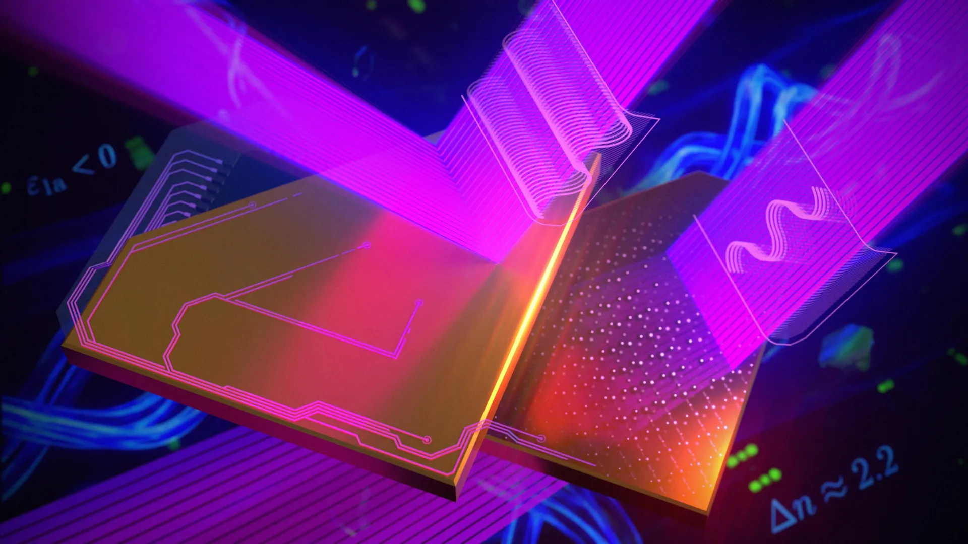
The Cambridge-led team utilized a two-dimensional electron gas (2DEG) trapped within a semiconductor heterostructure. In this environment, electrons are confined to a plane only a few nanometers thick, behaving as a high-mobility fluid. When terahertz photons strike this 2DEG, they transfer their energy to the electrons. Instead of being ejected from the material, these energized electrons cross a "potential step"—a small, tunable barrier created within the plane of the semiconductor. This movement generates a measurable electrical current.
Because the entire process occurs "in-plane," it eliminates the need for electrons to travel across thick material layers, reducing the likelihood of energy loss and increasing the speed of the response. However, early versions of PETS detectors suffered from poor light absorption; because the active detection region was so small, most of the incoming terahertz radiation simply passed by without interacting with the electrons.
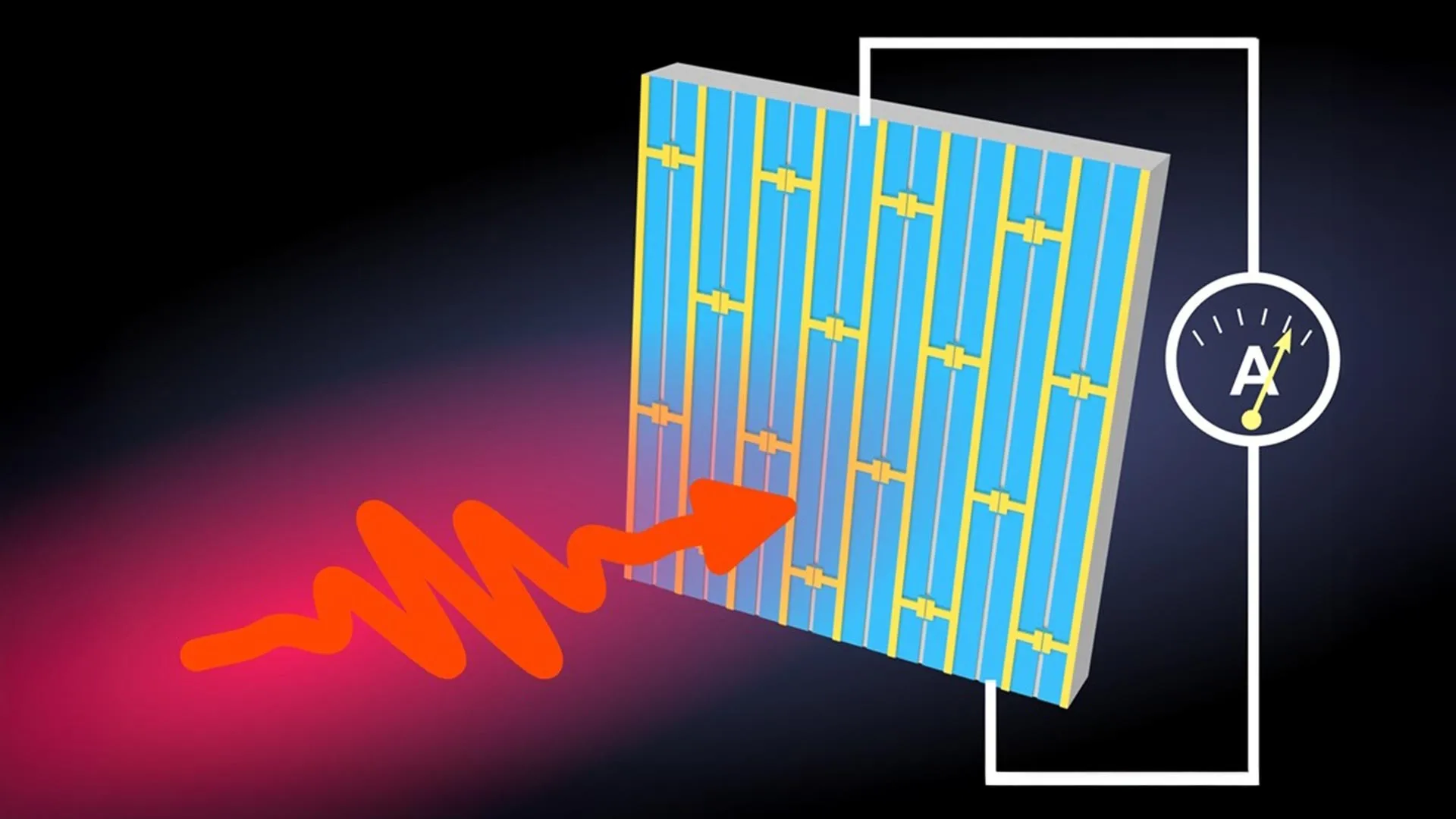
Engineering the "Brickwork" Metasurface
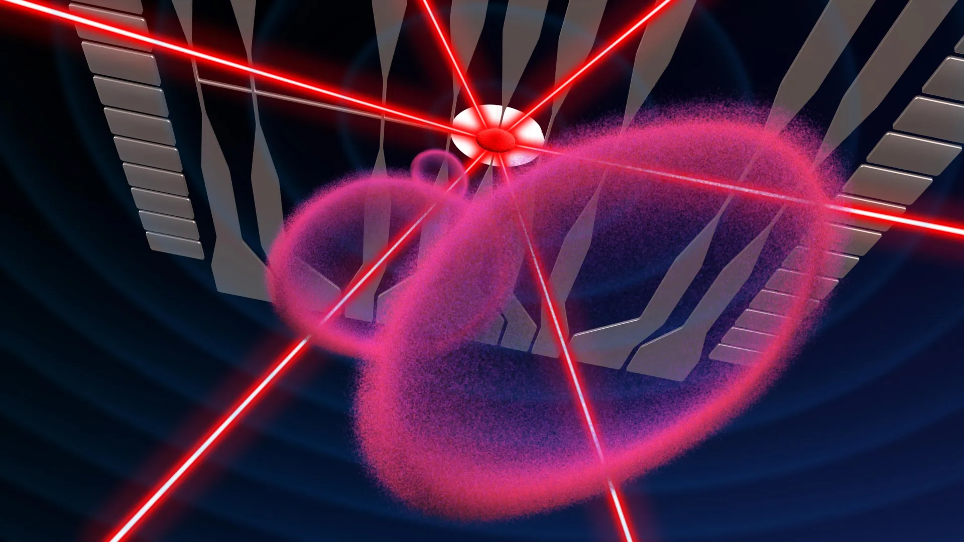
To solve the absorption problem, the researchers turned to the field of metasurfaces—artificial materials engineered to have properties not found in nature. They designed a metallic metasurface featuring a repeating "brickwork" pattern. This structure acts as a sophisticated antenna array that captures incoming terahertz waves from a large area and "squeezes" them into extremely narrow capacitive gaps.
These gaps are where the PETS detection elements are located. By embedding the quantum detection mechanism directly into the regions of highest electric field enhancement, the team ensured that nearly every captured photon had a high probability of generating a signal. This design represents a departure from traditional detector architecture, where the light-gathering optics (such as bulky silicon lenses) are separate from the sensing element.
The metasurface serves a dual purpose: it acts as both the optical concentrator and the electrical contact for the device. The researchers used advanced computer simulations to optimize the geometry of the brickwork, balancing the need for tight field confinement with the requirement for a wide enough channel to allow electron flow. This optimization led to a design where the electric field strength in the gaps is orders of magnitude higher than that of the incident radiation.
Experimental Results and Performance Metrics
The prototype device was fabricated using high-mobility gallium arsenide (GaAs) and aluminum gallium arsenide (AlGaAs) heterostructures, a staple of modern semiconductor physics. Testing was conducted at a temperature of 10 K to characterize the fundamental physics of the device, although the researchers noted that the technology is theoretically capable of operating at higher temperatures achievable with compact, closed-cycle cryocoolers.
When exposed to radiation at 1.9 THz, the detector demonstrated a responsivity of 2.7 amperes per watt (A/W). More significantly, the external quantum efficiency (EQE)—a measure of how many incident photons are successfully converted into electrons in the output current—was measured at 2.1 percent. While a few percent might seem low in the context of visible-light sensors, in the terahertz regime, this represents a twenty-fold (2,000%) improvement over previous PETS detectors that did not utilize metasurfaces.
Furthermore, the detector operates at "zero bias," meaning it does not require an external voltage to be applied across the source and drain to function. This is a major advantage for sensitivity, as it eliminates "dark current"—the background noise created by flowing electricity that can drown out weak signals.
Implications for 6G and Beyond
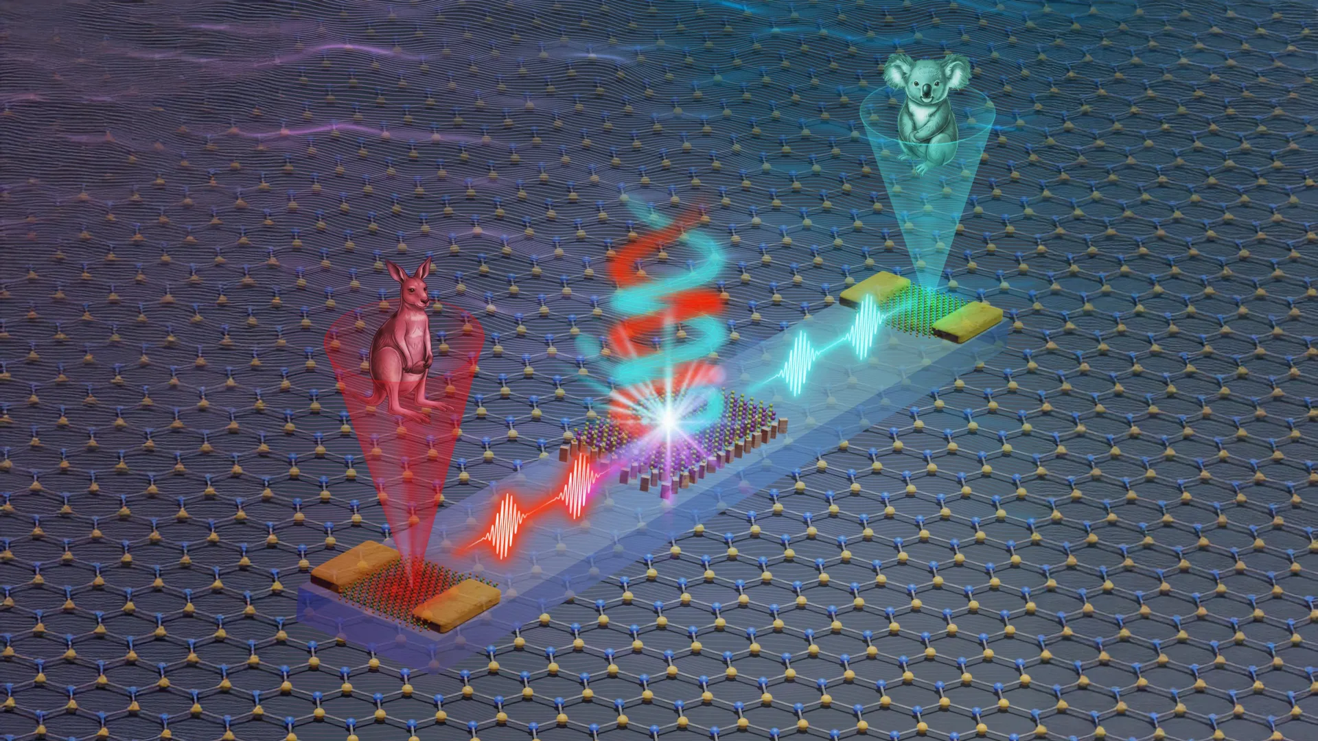
The implications of this research extend far beyond the laboratory. One of the most anticipated applications is in the development of 6G wireless networks. As global data demand continues to surge, telecommunications companies are looking toward terahertz frequencies to provide the bandwidth necessary for multi-terabit-per-second transmission. Compact, efficient detectors that can be integrated onto semiconductor chips are essential for the hardware that will power these future networks.
In the medical field, terahertz radiation is highly valued because it is non-ionizing, meaning it does not damage biological tissue like X-rays do. It is also highly sensitive to water content, making it an ideal tool for detecting skin cancers or monitoring hydration levels in wounds. The ability to create flat, "lens-free" detectors could lead to portable terahertz imaging wands for use in clinical settings.
Industrial quality assurance is another sector poised for disruption. Terahertz waves can penetrate many common materials like plastics, ceramics, and clothing, but are reflected by metals and absorbed by moisture. This allows for the non-destructive inspection of packaged goods, the detection of hidden defects in composite materials used in aerospace, and the identification of illicit substances in security screening.
Chronology and Research Collaboration
The development of this detector is the result of a multi-year collaboration between leading UK institutions. The initial concept for the PETS detector was developed within the Semiconductor Physics Group at the Cavendish Laboratory, University of Cambridge. Lead researcher Wladislaw Michailow, who transitioned from Cambridge to Swansea University during the project, spearheaded the integration of the metasurface.
Ruqiao Xia, the study’s first author, performed the intricate fabrication and measurement of the devices during her doctoral research at Cambridge. The project was overseen by Professor David Ritchie, a prominent figure in semiconductor research who has spent decades advancing the capabilities of 2D electron systems.
The timeline of the research reflects a steady progression from fundamental quantum discovery to applied engineering:
- Early 2020s: Validation of the in-plane photoelectric effect in 2DEG systems.
- 2021-2022: Identification of low light-coupling efficiency as the primary bottleneck for PETS detectors.
- 2023: Design and simulation of the "brickwork" metasurface to enhance field concentration.
- 2024: Successful fabrication and testing of the integrated quantum metasurface detector, culminating in the Advanced Photonics publication.
Conclusion and Future Directions
The integration of metasurface optics with quantum-well physics represents a paradigm shift in how scientists approach the terahertz gap. By moving away from bulky external components and focusing on "on-chip" light manipulation, the Cambridge and Swansea team has provided a blueprint for the next generation of electromagnetic sensors.
Future work will likely focus on increasing the operating temperature of the device. While 10 K is suitable for astronomical observations (where detectors are often cooled to even lower temperatures), terrestrial applications in healthcare and telecommunications would benefit from room-temperature operation or cooling provided by small, solid-state Peltier elements. Given that the PETS mechanism is geometrically scalable, the researchers believe the design can be tuned for various frequencies, potentially covering the entire range from microwaves to the mid-infrared.
As Professor David Ritchie noted, the versatility of the platform is its greatest strength. By combining the precision of quantum mechanics with the flexibility of metasurface engineering, the "terahertz gap" is finally being bridged, opening the door to a new era of wireless sensing and communication.