
Electrical engineers at Duke University have achieved a significant breakthrough in the field of optoelectronics by demonstrating the fastest pyroelectric photodetector ever recorded. This novel device, which identifies light by sensing the infinitesimal amounts of heat generated upon absorption, operates at speeds previously thought impossible for thermal-based sensors. By integrating advanced plasmonic metasurfaces with ultra-thin pyroelectric materials, the research team has developed a sensor capable of responding to light in just 125 picoseconds—a performance metric that rivals conventional silicon-based semiconductor detectors while offering a significantly broader spectral range.
The findings, recently published in the prestigious journal Advanced Functional Materials, mark a departure from the traditional trade-offs in sensor design, where sensitivity and speed are often at odds. This technology operates efficiently at room temperature, requires no external bias or power source to function, and is designed for seamless integration into modern on-chip systems. As the demand for compact, high-speed multispectral imaging grows, this development stands to revolutionize sectors ranging from autonomous vehicle navigation and satellite-based remote sensing to non-invasive medical diagnostics and precision agriculture.
The Technological Barrier: Semiconductors vs. Thermal Detectors
To understand the magnitude of the Duke University achievement, it is necessary to examine the limitations inherent in current imaging technologies. Most contemporary digital cameras and optical sensors rely on semiconductor-based photodetectors. These devices work through the photoelectric effect: when photons of a specific energy level strike the semiconductor material, they excite electrons, creating an electrical current that a computer processes into a digital image.
However, semiconductors are fundamentally limited by their "bandgap"—the specific energy threshold required to excite an electron. This means that a standard silicon sensor is essentially "blind" to large portions of the electromagnetic spectrum, particularly the infrared and ultraviolet regions, much like the human eye. To capture light outside the visible spectrum, engineers have historically turned to thermal detectors, such as bolometers or pyroelectric sensors.
Pyroelectric detectors operate on a different physical principle. They utilize materials that naturally possess a permanent electrical polarization. When these materials absorb light and experience even a marginal increase in temperature, their internal polarization changes, producing a measurable electrical signal. While these sensors are prized for their ability to detect a wide array of wavelengths—from long-wave infrared to ultraviolet—they have traditionally been plagued by slow response times. Because heat dissipation and thermal mass usually dictate the speed of these devices, commercial pyroelectric sensors typically operate in the microsecond or millisecond range, making them unsuitable for high-speed applications or video-rate imaging.
The Engineering Breakthrough: Plasmonic Metasurfaces
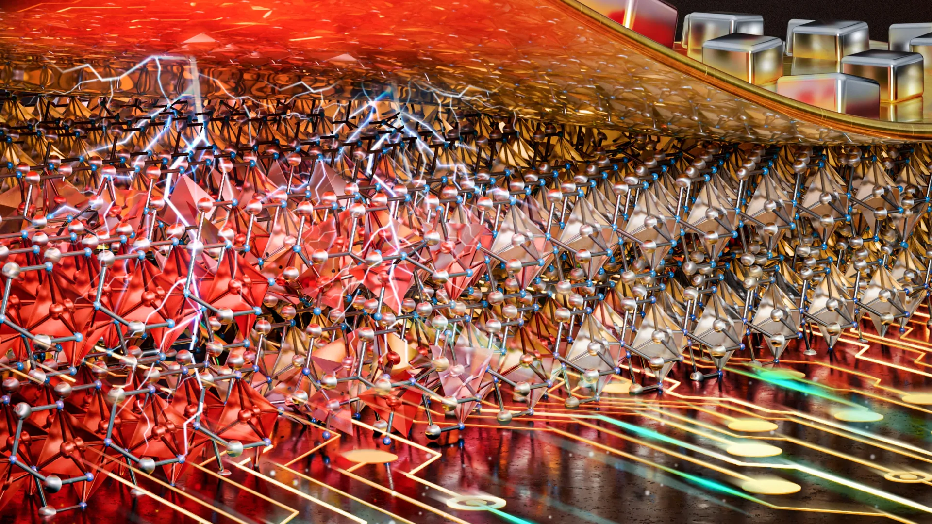
The research team, led by Maiken Mikkelsen, a professor of electrical and computer engineering at Duke, addressed the speed bottleneck by reimagining the architecture of the detector. The core of their innovation lies in a "metasurface"—a synthetic structure engineered to have optical properties not found in nature.
The Duke metasurface consists of an array of silver nanocubes precisely positioned just 10 nanometers above a thin, continuous sheet of gold. Separating these two metallic layers is a transparent spacer and a super-thin layer of pyroelectric material. When light strikes this structure, it triggers a phenomenon known as plasmonics. The nanocubes act as tiny antennas, capturing the energy of the incoming photons and confining it into the 10-nanometer gap between the cubes and the gold film.
This intense confinement of light allows for nearly 100% absorption within an incredibly small volume. Because the light is trapped so efficiently, the device requires only a negligible amount of pyroelectric material to generate a signal. This reduction in thermal mass is the primary driver behind the device’s unprecedented speed. By minimizing the amount of material that needs to be heated, the researchers effectively bypassed the slow thermal diffusion processes that limit traditional detectors.
"Commercial pyroelectric detectors aren’t very responsive, so they need a very bright light or very thick absorbers to work, which naturally makes them slow because heat doesn’t move that fast," Professor Mikkelsen explained. "Our approach cleverly integrates near-perfect absorbers and super-thin pyroelectrics to achieve a response time of 125 picoseconds, which is a huge improvement for the field."
A Chronology of Development and Optimization
The journey toward this record-breaking speed began in 2019, when Mikkelsen’s laboratory first demonstrated the proof-of-concept for a metasurface-enhanced pyroelectric detector. While that initial version proved that the physics of light trapping worked, it was not optimized for speed, and the team lacked the specialized equipment to measure response times in the picosecond regime.
Over the subsequent years, the focus shifted toward refinement and high-frequency optimization. Eunso Shin, a PhD student in Mikkelsen’s lab and the lead author of the study, spearheaded the effort to redesign the device for maximum throughput. One of the most significant changes was the transition from a rectangular metasurface layout to a circular configuration. This geometric shift increased the effective surface area for light collection while simultaneously shortening the path that electrical signals had to travel to reach the readout electronics, thereby reducing parasitic capacitance and inductance.
To validate the device’s performance, the team had to innovate in the realm of experimental measurement. Shin developed a sophisticated setup utilizing two distributed feedback lasers. By overlapping the frequencies of these lasers, the researchers created a "beat frequency" that could be modulated at extremely high speeds. When the frequency of the light modulation approached the operating speed of the detector, the researchers could precisely map the device’s response curve.
Supporting Data: Achieving Gigahertz Speeds
The results of these experiments exceeded the team’s initial expectations. The measurements revealed that the thermal photodetector could operate at frequencies up to 2.8 GHz. In practical terms, this means the sensor can produce a distinct electrical signal in just 125 picoseconds after being struck by light.
When compared to existing technology, the data highlights a generational leap:
- Traditional Pyroelectric Sensors: Typical response times range from 10 microseconds to 1 millisecond.
- Duke Plasmonic Detector: Response time of 0.000125 microseconds (125 picoseconds).
- Improvement Factor: The new device is approximately 1,000 to 10,000 times faster than commercial thermal detectors.
Furthermore, because the metasurface can be "tuned" by changing the size and spacing of the silver nanocubes, the detector can be customized to target specific wavelengths without changing the base materials. This flexibility, combined with its high speed, places the pyroelectric detector in a performance bracket previously occupied exclusively by high-end semiconductor photodetectors, which often require cryogenic cooling to achieve similar results in the infrared spectrum.
Official Responses and Scientific Implications
The reaction from the researchers reflects the disruptive potential of the discovery. Maiken Mikkelsen noted that the results challenge the long-held assumption that thermal detectors are inherently slow. "Thermal photodetectors are supposed to be slow, so this was mind-boggling to the entire community," she said. "We were taken off guard that it seemed to be working on time scales similar to that of silicon photodetectors."
Eunso Shin emphasized that while the 2.8 GHz mark is a milestone, it may not be the ultimate ceiling for this technology. "Pyroelectric photodetectors commonly operate in the nano-to-microsecond range, so this is hundreds or thousands of times faster," Shin said. "These results are really exciting, but we’re still working to make them even faster while figuring out the kinetic limit of pyroelectric photodetectors."
The broader scientific community views this as a significant step toward "on-chip" multispectral sensing. By integrating these detectors directly into CMOS (Complementary Metal-Oxide-Semiconductor) circuits, manufacturers could produce cameras that see not just color, but the "chemical fingerprint" of objects based on their infrared signatures, all on a single, low-power chip.
Broader Impact: From Precision Agriculture to Oncology
The practical applications for a high-speed, uncooled, and self-powered multispectral detector are vast. In the field of medicine, the technology could lead to the development of handheld devices for skin cancer screening. Since cancerous tissues often exhibit different metabolic rates and thermal profiles than healthy tissue, a high-speed multispectral camera could identify suspicious lesions with greater accuracy than the naked eye or standard photography.
In the agricultural sector, the technology holds promise for "precision farming." Current multispectral sensors used in agriculture are often bulky and expensive, requiring significant power from the drones or tractors that carry them. The Duke-developed sensors, which require no external power to generate a signal, could be deployed in massive, low-cost sensor networks or on lightweight drones to monitor crop health. By detecting specific wavelengths associated with water stress or nutrient deficiency, these sensors could tell a farmer exactly which square meter of a field requires attention, drastically reducing the use of water and fertilizer.
The aerospace and defense industries are also likely to take interest. Because the detectors are ultrathin and require no cooling, they are ideal candidates for use in small satellites (CubeSats) and deep-space probes where weight and power consumption are critical constraints. These sensors could facilitate real-time monitoring of atmospheric gases, greenhouse gas emissions, or even the detection of distant celestial bodies in wavelengths that current small-scale sensors cannot reach.
Future Research and Commercialization
Moving forward, the Duke research team is exploring ways to push the speed limits even further. One proposed method involves placing the pyroelectric material and the electronic readout components directly into the 10-nanometer gap between the nanocubes and the gold layer. This would further reduce signal latency and potentially push the device into the tens of gigahertz range.
Additionally, the team is working on "multiplexed" designs. By placing different sizes of nanocubes on a single chip, they can create a sensor array where each pixel is sensitive to a different wavelength or polarity of light. This would allow for the creation of a truly "universal" camera capable of capturing the entire electromagnetic spectrum simultaneously.
The research was made possible through support from the Air Force Office of Scientific Research and the Gordon and Betty Moore Foundation. As the team addresses the challenges of large-scale manufacturing and integration, the transition from a laboratory record to a commercial standard appears increasingly likely. While the researchers admit that widespread commercial use is "down the line," the fundamental barriers to high-speed thermal imaging have effectively been dismantled.


Leave a Reply