

The global transition toward renewable energy has long been anchored by silicon-based photovoltaics, a technology that has benefited from over half a century of refinement, massive industrial scaling, and rigorous purification processes. However, a disruptive class of materials known as lead-halide perovskites has rapidly closed the efficiency gap, achieving in just over a decade what took silicon five decades to accomplish. The central mystery of this ascent has been how a material produced through relatively crude, low-cost solution processing—riddled with structural flaws and impurities—could perform as well as ultra-pure, single-crystal silicon. A landmark study recently published in Nature Communications by researchers at the Institute of Science and Technology Austria (ISTA) has finally provided the physical explanation for this phenomenon, revealing that the very defects once thought to be hindrances are, in fact, the secret to the material’s success.
The Perovskite Paradox: Efficiency Amidst Imperfection
In the world of semiconductors, "purity" is usually synonymous with "performance." For a standard silicon solar cell to function, the silicon must be refined to "solar grade" purity, often exceeding 99.9999%. Any structural break in the crystal lattice or the presence of foreign atoms acts as a "trap," capturing electrical charges and preventing them from reaching the electrodes. This recombination of charges results in energy loss and reduced efficiency.
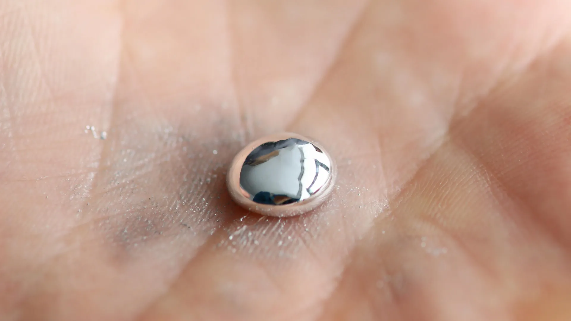
Lead-halide perovskites defy this fundamental logic. These materials are hybrid organic-inorganic compounds that can be manufactured using simple chemical "soups" at room temperature. The resulting crystals are inherently "messy," filled with dislocations and chemical irregularities. Despite this, perovskites demonstrate extraordinary charge-carrier lifetimes and long diffusion lengths. Scientists Dmytro Rak and Zhanybek Alpichshev at ISTA set out to investigate why these "dirty" materials do not suffer from the massive energy losses seen in other imperfect semiconductors. Their research confirms that perovskites possess a unique internal architecture that actively facilitates charge transport rather than hindering it.
A Chronology of the Perovskite Revolution
The rise of perovskites is one of the fastest-moving narratives in modern materials science. To understand the significance of the ISTA discovery, it is essential to look at the timeline of the material’s evolution:
- 1839: The original mineral perovskite (calcium titanate) is discovered in the Ural Mountains by Gustav Rose and named after Russian mineralogist Lev Perovski.
- 1970s: Scientists first synthesize lead-halide versions of the perovskite structure. At the time, they are viewed as academic curiosities with interesting crystalline properties but no clear application.
- 2009: The first perovskite solar cell is reported by Tsutomu Miyasaka’s team, yielding an efficiency of just 3.8%. The cell is unstable and dissolves in the liquid electrolyte.
- 2012: A breakthrough occurs as researchers replace the liquid electrolyte with a solid-state hole transporter, pushing efficiency over 10% and improving stability.
- 2015–2020: Efficiency rates skyrocket, surpassing 20%. Perovskites begin to be integrated with silicon in "tandem cells," which aim to break the theoretical efficiency limits of single-junction silicon.
- 2024: The ISTA study provides the first comprehensive physical model explaining the internal mechanics of charge separation within these crystals, solving the "mystery of efficiency" that has persisted for 15 years.
The Discovery of Charge Highways
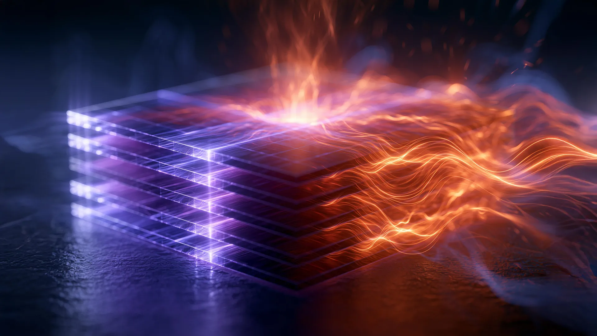
The core of the ISTA team’s findings lies in the discovery of "domain walls." In lead-halide perovskites, the crystal structure is not a single, uniform block. Instead, it is composed of different regions where the crystal lattice is oriented in slightly different directions. The boundaries between these regions are known as domain walls.
Previously, these walls were often viewed as defects that might scatter charges. However, Rak and Alpichshev discovered that these domain walls act as "highways" for electrical charges. When sunlight hits the perovskite, it creates negatively charged electrons and positively charged "holes." In most materials, these opposite charges are attracted to one another and recombine, wasting the energy as heat.
Within the perovskite, however, the researchers found that internal electric fields exist at these domain walls. These fields act like a centrifugal force, pulling the electrons and holes in opposite directions. Once separated, the charges are trapped on either side of the wall, preventing them from recombining. They are then free to travel along these interconnected "highways" over vast distances—hundreds of microns—to the electrodes. On the scale of a charge carrier, this distance is equivalent to a human traveling hundreds of kilometers without hitting a single roadblock.
Innovative Methodology: Visualizing the Invisible
One of the primary reasons this mechanism remained hidden for so long is the difficulty of observing the interior of a crystal. Traditional microscopy techniques often only capture surface-level data, which does not accurately reflect the complex 3D network of domain walls deep inside the material.
To solve this, Dmytro Rak utilized his background in chemistry to develop a technique reminiscent of medical angiography. In medicine, doctors inject a contrast agent into the bloodstream to visualize veins and arteries on an X-ray. Rak applied this logic to the perovskite crystal. Since perovskites are ionic conductors, he introduced silver ions into the material. These ions naturally migrated toward the internal domain walls, accumulating along the structural boundaries.
Once the silver ions were in place, the researchers used a chemical process to convert them into metallic silver. This effectively "stained" the internal highways of the crystal. Under a microscope, a dense, intricate network of domain walls became visible for the first time. This qualitative visualization provided the "smoking gun" evidence that these internal structures were pervasive and interconnected throughout the entire crystal volume.
Comparative Data and Technical Implications
The implications of this discovery are best understood through a comparison of perovskite performance metrics against traditional silicon technology.
| Feature | Silicon (Monocrystalline) | Lead-Halide Perovskites |
|---|---|---|
| Manufacturing Temp | ~1,400°C | Room Temperature to 150°C |
| Purity Requirement | >99.9999% | Moderate (Solution-based) |
| Charge Separation | Requires P-N junction engineering | Natural (Internal Domain Walls) |
| Efficiency (Lab) | ~26.7% | ~26.1% (Rapidly increasing) |
| Cost of Production | High (Energy-intensive) | Low (Printable/Spin-coated) |
| Flexibility | Rigid/Brittle | Flexible/Thin-film |
The ISTA study clarifies why perovskites can achieve silicon-like efficiency without the energy-intensive purification. By utilizing the naturally occurring domain walls as charge separators, the material effectively does the hard work of energy conversion "for free" as a result of its own structural imperfections.
Scientific and Industry Reactions
The publication has sparked significant interest across the materials science community. While the study is fundamentally a piece of basic research, its practical implications for the solar industry are profound.
Dr. Alpichshev noted that the findings reconcile years of conflicting data. "For a long time, researchers were seeing these amazing properties—long charge lifetimes and high mobility—but couldn’t explain how they coexisted with such a high density of defects. Our work provides a unified physical framework that accounts for almost all documented properties of these materials."
Industry analysts suggest that this understanding could pivot the focus of perovskite research. Currently, most efforts to improve the material focus on chemical additives to "passivate" or heal defects. However, if defects (in the form of domain walls) are actually the engines of efficiency, the goal may shift toward "defect engineering"—purposefully designing the network of domain walls to optimize the flow of electricity.
Broader Impact and Future Applications
Beyond solar energy, the ISTA team’s discovery has implications for other optoelectronic technologies. Because perovskites are highly efficient at both absorbing and emitting light, they are being developed for:
- Next-Generation LEDs: The same "highways" that transport charges in solar cells can be used to transport injected charges to specific points for highly efficient light emission, potentially leading to cheaper and more vibrant displays.
- Medical Imaging: Perovskites are exceptionally sensitive to X-rays. This new understanding of charge transport could lead to ultra-low-dose X-ray detectors, reducing radiation exposure for patients.
- Quantum Computing: Alpichshev’s group is particularly interested in the "quantum coherence" observed in these materials at room temperature. The ability of charges to remain "coherent" or synchronized while traveling along domain walls could open new avenues for quantum information processing.
Conclusion: A New Era for Photovoltaics
The work of Rak and Alpichshev marks a turning point in the study of lead-halide perovskites. By proving that internal structural defects form a functional network of "highways" for electricity, the ISTA researchers have dismantled the long-standing belief that semiconductor efficiency requires near-perfect crystalline purity.
As the solar industry looks toward 2030 and beyond, the focus will increasingly shift from "how" these materials work to "how" they can be stabilized for decades of use in the field. With the physical mechanism of their efficiency now laid bare, scientists have the roadmap they need to move perovskite solar cells out of the laboratory and onto the world’s rooftops, potentially providing a cheaper, more accessible path to global decarbonization.


Leave a Reply