

In a significant advancement for the field of materials science, a research team at the University of California, Davis, has documented a remarkable and previously misunderstood property within a class of materials known as halide perovskites. According to a study published on March 3 in the prestigious journal Advanced Materials, these crystals possess the ability to undergo rapid, reversible structural deformations when exposed to light—a phenomenon known as photostriction. Unlike traditional semiconductors such as silicon or gallium arsenide, which maintain a rigid atomic lattice under illumination, halide perovskites shift their internal geometry in response to photons and return to their original state once the light source is removed. This discovery suggests a future where electronic components are not merely powered by electricity but are mechanically and structurally tuned by light, offering a new frontier for sensors, actuators, and high-speed communication technologies.
The Evolution of Semiconductor Materials: From Silicon to Perovskites
For over half a century, the electronics industry has been dominated by silicon. While silicon’s stability and abundance made it the backbone of the digital age, its rigid crystalline structure limits its versatility in emerging fields like flexible electronics and light-controlled mechanical systems. Gallium arsenide (GaAs) offered improvements in electron mobility and light emission, yet both materials remain fundamentally "static" in their physical dimensions during operation.
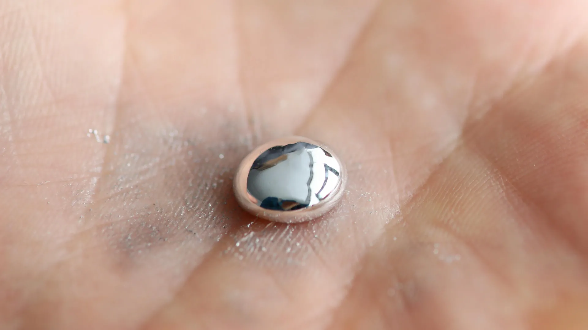
Perovskites, named after the 19th-century Russian mineralogist Lev Perovski, represent a radical departure from these traditional materials. While the term originally referred to calcium titanate ($CaTiO_3$), it now describes a broad class of compounds sharing the $ABX_3$ crystal structure. In this arrangement, a central atom (B) is surrounded by an octahedron of six atoms (X), all of which are housed within a larger cube defined by atoms at the corners (A). Halide perovskites, which utilize halogen elements like iodine, bromine, or chlorine in the "X" position, have gained global attention over the last decade primarily for their extraordinary efficiency in converting sunlight into electricity.
Marina Leite, a professor of materials science engineering at UC Davis and the senior author of the study, describes perovskites as "smart materials." According to Leite, these substances can be precisely engineered to respond to specific external stimuli. The research highlights that the chemistry of halide perovskites is uniquely flexible, allowing for the creation of devices that were previously considered impossible with the rigid constraints of traditional solid-state physics.
Experimental Methodology and the Role of Photostriction
The breakthrough was the result of an international collaboration between UC Davis and researchers at ETH Zürich in Switzerland. The Swiss team, including Bekir Turedi, Andrii Kanak, and Professor Maksym Kovalenko, provided high-quality perovskite crystals necessary for the high-precision measurements. Mansha Dubey, a graduate student in Leite’s lab, led the experimental phase, which involved directing focused laser light onto the crystals while simultaneously monitoring their atomic lattice using X-ray diffraction techniques.
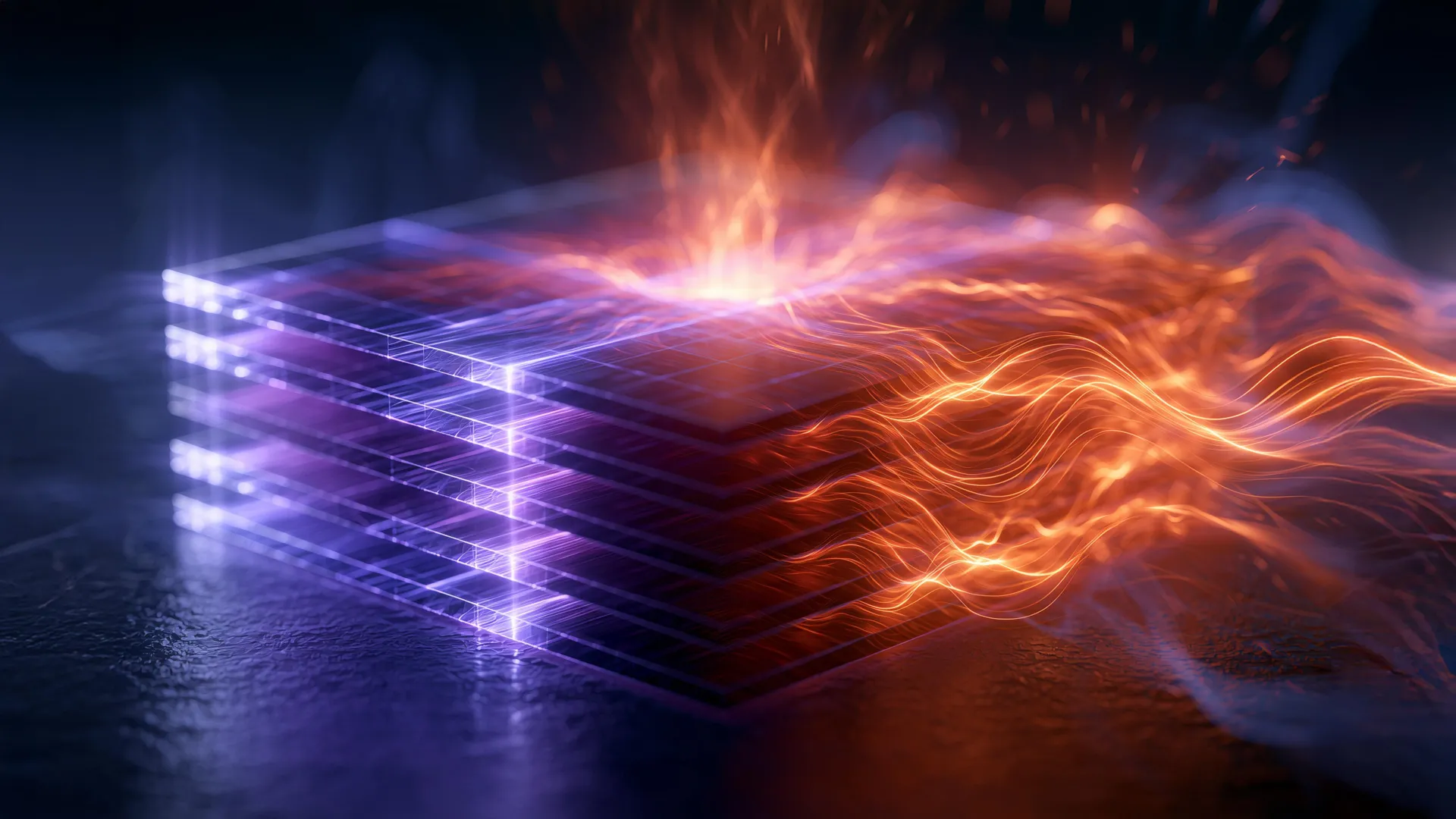
The X-ray measurements allowed the team to observe the "breathing" of the crystal lattice in real-time. When the laser hit the material, the atoms shifted, causing the lattice to expand or contract—a physical manifestation of photostriction. Photostriction is a process where light energy is converted directly into mechanical strain. While this effect has been observed in certain ferroelectric materials, seeing it in a semiconductor with such speed and reversibility is rare.
The data revealed that the change was not a permanent degradation or a thermal expansion caused by heat. Instead, it was a purely photo-induced quantum mechanical response. Once the laser was deactivated, the crystals snapped back to their original configuration. This cycle was repeated numerous times without any evidence of material fatigue, suggesting that halide perovskites could be used in high-frequency switching applications where durability is paramount.
Technical Analysis: The "Dimmer Switch" Effect and Bandgap Tunability
One of the most compelling findings of the UC Davis study is the "tunable" nature of the response. In traditional electronics, signals are often binary—on or off, high or low. However, the photostriction in halide perovskites behaves more like a dimmer switch. The researchers found that the magnitude of the shape change is directly proportional to both the intensity and the wavelength (color) of the light applied.
This behavior is tied to the material’s "bandgap"—the energy threshold required to excite an electron into a state where it can conduct electricity. By altering the chemical composition of the perovskite (for example, by swapping iodine for bromine), scientists can shift this bandgap. The UC Davis team discovered that the structural response is particularly sensitive at frequencies just above the bandgap. This level of control allows for a "scaled response," where the physical displacement of the crystal can be modulated with extreme precision by simply adjusting the brightness of a light source.
Supporting data from the study indicates that the lattice strain observed is significantly higher than what is typically seen in other light-responsive materials. This high degree of "strain-per-photon" makes perovskites an ideal candidate for opto-mechanical transducers, which convert optical signals into mechanical movement.
Chronology of the Discovery and Institutional Support
The journey toward this discovery began several years ago as researchers worldwide noticed "anomalous" behaviors in perovskite solar cells, such as hysteresis and unexpected fluctuations in efficiency. The UC Davis team hypothesized that these anomalies were not defects, but rather intrinsic properties of the material’s flexible lattice.
The timeline of the research involved several phases:
- Synthesis Phase (2022-2023): Collaborative efforts with ETH Zürich to produce ultra-pure halide perovskite crystals that could withstand rigorous X-ray analysis.
- Characterization Phase (Mid-2023): Utilization of the UC Davis Advanced Materials Characterization and Testing (AMCaT) laboratory. This facility, established with support from the National Science Foundation (NSF), provided the instrumentation necessary to observe atomic-scale movements.
- Data Validation (Late 2023): Repeated testing to confirm that the lattice shifts were reversible and not the result of heat-induced expansion.
- Publication (March 2024): Formal presentation of the findings in Advanced Materials, establishing a new framework for light-matter interaction in semiconductors.
The research was heavily supported by the federal Defense Advanced Research Projects Agency (DARPA). DARPA’s interest stems from the potential for "switchable photonic devices"—components that can change their optical properties on the fly, which are vital for advanced radar, secure communications, and stealth technologies.
Broader Implications and Future Applications
The implications of this research extend far beyond the laboratory. By understanding how to manipulate the shape of a semiconductor with light, engineers can begin to design a new class of "wireless" actuators. Currently, most mechanical actuators in robotics or micro-electromechanical systems (MEMS) require complex wiring to deliver electrical pulses. Light-controlled perovskites could allow for remote, non-contact manipulation of mechanical parts using fiber optics or directed lasers.
Furthermore, the discovery has significant ramifications for the future of solar energy. One of the primary hurdles for perovskite solar cells has been their long-term stability. Understanding that the lattice "moves" under sunlight is crucial for developing better packaging and chemical formulations that can accommodate this movement without cracking or degrading over time.
In the realm of telecommunications, light-induced shape-shifting could lead to new types of optical switches. As global data demands increase, the ability to switch optical signals mechanically at the atomic level could reduce the energy consumption of data centers, which currently rely on power-hungry electronic conversion.
Industry and Academic Perspectives
While the UC Davis team remains focused on the fundamental physics, the broader scientific community has reacted with cautious optimism. Independent analysts suggest that if the reversibility and speed of this photostriction can be maintained at a commercial scale, halide perovskites could challenge the dominance of silicon in niche markets, particularly in aerospace and medical imaging.
However, challenges remain. Halide perovskites are notoriously sensitive to moisture and oxygen. For these light-controlled devices to become a reality in consumer electronics, the industry must develop robust encapsulation techniques to protect the "breathing" crystals from environmental degradation.
The UC Davis study marks a pivotal shift in how scientists view semiconductors. No longer are they seen as static platforms for electron flow; instead, they are becoming dynamic, responsive systems. As Professor Leite and her team continue to explore the limits of these "smart materials," the boundary between optics, mechanics, and electronics continues to blur, promising a future of technology that is literally shaped by light.


Leave a Reply