
The detection of electromagnetic radiation across various spectra serves as the backbone of modern technological infrastructure, facilitating everything from fiber-optic telecommunications to medical imaging and deep-space astronomy. However, a persistent "gap" has long existed in the terahertz (THz) range, a region of the electromagnetic spectrum nestled between the high-frequency end of microwaves and the low-frequency edge of infrared light. For decades, the terahertz range—typically defined as frequencies between 0.1 and 10 THz—has remained notoriously difficult to harness. Existing detection technologies for these frequencies have historically been plagued by a "triple threat" of limitations: they are often prohibitively slow, lack the necessary sensitivity for practical field use, or require massive, expensive cryogenic cooling systems to function.
A significant leap toward bridging this gap has been achieved by a multi-institutional research team. By synthesizing principles of quantum physics with advanced metasurface engineering, researchers have developed a compact, high-performance detector capable of capturing and converting terahertz radiation into electrical signals with unprecedented efficiency. The study, recently published in the journal Advanced Photonics, details a device architecture that addresses the fundamental physics of photon-to-electron conversion, offering a twenty-fold improvement in external quantum efficiency over previous iterations of similar technology.
The Challenge of the Terahertz Gap
The terahertz region is often referred to as the "forgotten" or "difficult" middle ground of the electromagnetic spectrum. In the lower microwave frequencies, electronic components like transistors and oscillators can easily manipulate signals. In the higher infrared and visible frequencies, optical methods and semiconductor bandgap engineering provide efficient tools for light detection. Terahertz radiation, however, falls into a regime where it is too high-frequency for traditional electronics to track and too low-energy for many standard optical sensors to detect without thermal noise overwhelming the signal.
Traditionally, terahertz detection has relied on bolometers, which measure the heat generated by absorbed radiation, or Schottky barrier diodes. While effective in controlled laboratory environments, bolometers are inherently slow due to their reliance on thermal changes, and many high-sensitivity versions require cooling to liquid helium temperatures (near absolute zero). Schottky diodes, while faster, struggle with sensitivity as frequencies increase toward the mid-infrared. The need for a fast, sensitive, and compact solution has become increasingly urgent as industries look toward the next generation of wireless communications (6G) and non-invasive medical diagnostics.
Evolution of the In-Plane Photoelectric Effect
The breakthrough device utilizes a sophisticated quantum mechanism known as the in-plane photoelectric effect (IPPE). To understand the significance of this, one must look at the standard photoelectric effect, for which Albert Einstein won the Nobel Prize. In the traditional effect, a photon strikes a material and provides enough energy for an electron to escape the material’s surface into a vacuum or another medium. This requires the photon to have a specific minimum energy, known as the work function.
In the terahertz range, photons carry very little energy—far less than what is needed to overcome the work function of most metals or the bandgap of most semiconductors. The in-plane photoelectric effect solves this by keeping the entire process within a two-dimensional electron gas (2DEG). Instead of escaping the material, electrons are energized within a single plane and forced to cross a "potential step"—a carefully engineered energy barrier within the semiconductor structure.
Earlier research into Photoelectric Tunable-Step (PETS) detectors proved that this concept could work. However, those early models were limited by their physical footprint. They relied on individual, isolated antenna elements to catch radiation. Because the wavelength of terahertz radiation is relatively large compared to the microscopic detection region, these single antennas captured only a tiny fraction of the available energy, leading to low overall efficiency.
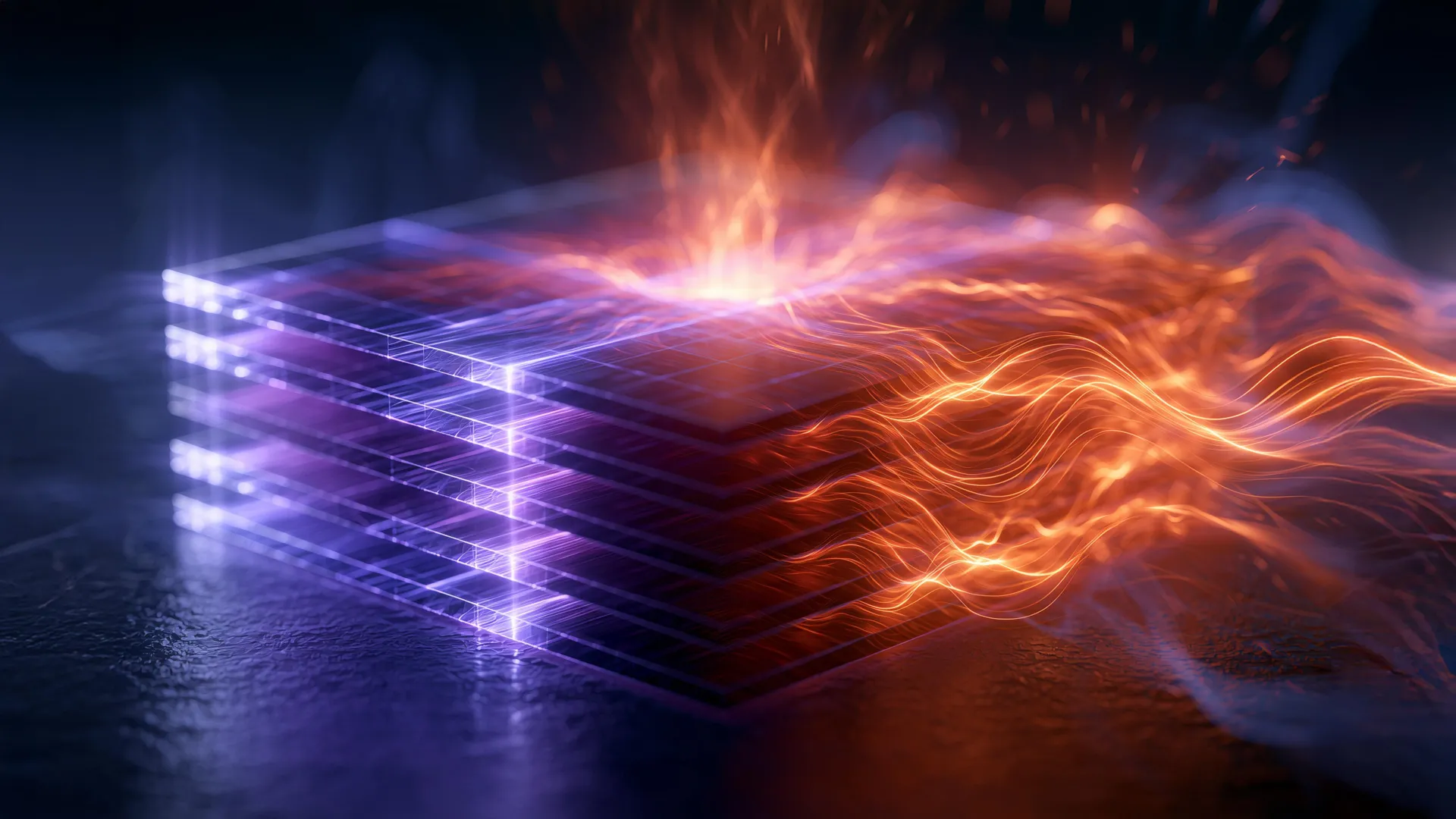
Engineering the Quantum Metasurface
To move beyond the limitations of single-antenna designs, the research team, led by Wladislaw Michailow of the University of Cambridge and later Swansea University, turned to metasurface engineering. A metasurface is an artificially structured interface featuring sub-wavelength patterns that can manipulate electromagnetic waves in ways natural materials cannot.
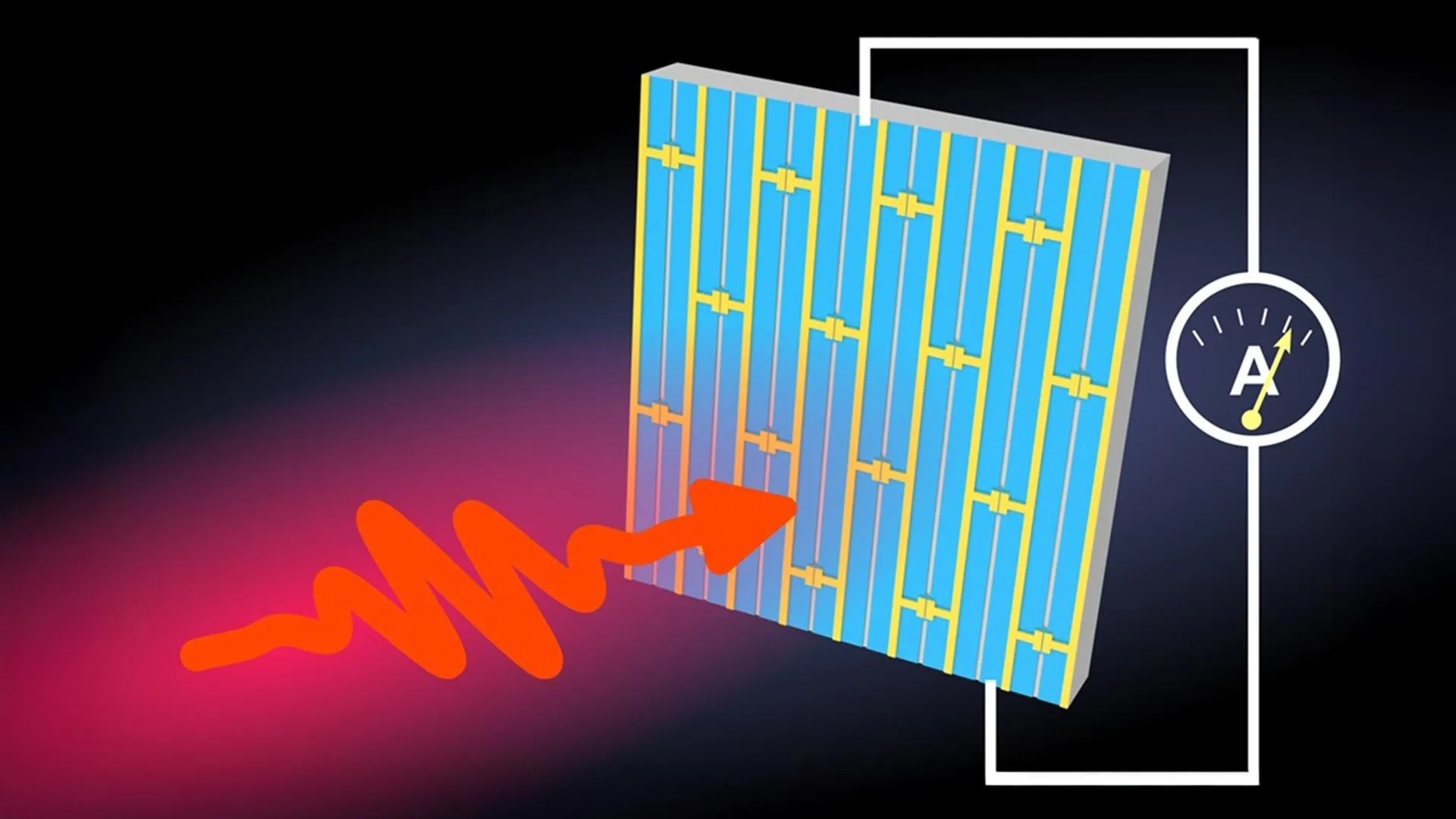
The team developed a "brickwork" metasurface pattern. This structure acts as a collective array of light-harvesting units. Rather than having a separate antenna and a separate detector, the metasurface is the detector. The design features narrow "capacitive gaps" between the brick-like structures. When terahertz radiation hits the metasurface, the patterned metal acts as a resonator, concentrating the electromagnetic field into these microscopic gaps.
This concentration is the key to the device’s performance. By channelling the energy into the exact regions where the 2D electron gas is located, the researchers ensured that nearly every captured photon had the maximum possible chance of interacting with an electron. This integrated approach removes the need for external focusing optics, such as bulky silicon lenses, which are standard in most current terahertz systems but add weight, cost, and alignment complexity.
Experimental Results and Performance Data
The researchers fabricated the detector using a high-mobility gallium arsenide (GaAs) and aluminum gallium arsenide (AlGaAs) heterostructure. This material system is a staple of high-frequency electronics and is compatible with existing semiconductor manufacturing processes, such as those used for field-effect transistors (FETs).
During testing, the device was cooled to 10 Kelvin (K) and exposed to radiation at 1.9 THz. The results showed a remarkable performance profile:
- Responsivity: The detector achieved a responsivity of 2.7 amperes per watt (A/W). This metric measures how much electrical current is produced for a given amount of incident light power.
- External Quantum Efficiency (EQE): The EQE reached 2.1 percent. While this number may seem small in the context of visible light sensors, it represents a twenty-fold (2,000%) improvement over previous PETS detectors operating in this frequency range.
- Zero-Bias Operation: One of the most significant technical advantages is that the detector operates at zero source-drain bias. In most sensors, a voltage must be applied to "read" the signal, which creates "dark current"—a background noise that exists even when no light is present. By operating at zero bias, this detector eliminates dark current, vastly improving the signal-to-noise ratio.
"The devices are direct detectors operating at zero bias, and therefore, they operate without dark currents," stated Ruqiao Xia, the study’s first author and a researcher at the Cavendish Laboratory. This characteristic is essential for detecting the incredibly faint signals often encountered in terahertz spectroscopy and astronomy.
Scalability and Integration
A critical aspect of this research is its "semiconductor-friendly" nature. Because the metasurface and the detection elements are fabricated using standard photolithography and etching techniques, the technology is inherently scalable.
The planar architecture means these detectors can be integrated directly onto chips alongside other electronic components, such as amplifiers and signal processors. Furthermore, the design is geometrically scalable. By simply changing the dimensions of the "brickwork" pattern and the gaps, the same physical principle can be applied to detect different frequencies, ranging from the microwave end of the spectrum all the way to the mid-infrared.
This flexibility suggests a path toward "multi-spectral" chips, where different regions of a single metasurface are tuned to different frequencies, allowing a device to "see" multiple parts of the terahertz spectrum simultaneously.
Future Implications and Industry Impact
The successful demonstration of a quantum metasurface photodetector based on a 2D electron system has wide-ranging implications across several high-tech sectors. David Ritchie, head of the Semiconductor Physics Group at the University of Cambridge, highlighted the breadth of these potential applications. "The results are particularly intriguing due to the applications that terahertz technology can enable," Ritchie noted, citing wireless networks, healthcare, and quality assurance in manufacturing.
Next-Generation Communications (6G)
As the world moves toward 6G technology, the demand for bandwidth is skyrocketing. Terahertz frequencies offer significantly more bandwidth than the radio waves used for 4G and 5G. However, 6G will require compact, highly sensitive detectors that can be integrated into mobile devices. This new metasurface detector provides a blueprint for the type of hardware needed to make ultra-high-speed terahertz communication a reality.
Medical and Biological Imaging
Terahertz radiation is non-ionizing, meaning it does not have the energy to damage DNA in the way X-rays do. However, it is highly sensitive to water content and molecular vibrations. This makes it ideal for detecting skin cancers, monitoring hydration levels in tissue, or performing "label-free" biological imaging where researchers can identify molecules without using fluorescent dyes.
Industrial Quality Control
In manufacturing, terahertz waves can penetrate many non-metallic materials like plastics, ceramics, and paper. This allows for real-time, non-destructive inspection of products. For instance, a terahertz sensor can "see" through a pill bottle to ensure tablets are correctly filled or inspect the integrity of ceramic coatings on turbine blades.
Astronomy and Spectroscopy
Terahertz detection is vital for understanding the cold universe. Many molecules in interstellar space emit signatures in the terahertz range. More efficient, compact detectors could lead to a new generation of portable spectrometers and satellite-based observatories that do not require massive liquid-helium cooling tanks, potentially extending the lifespan and reducing the cost of space missions.
Towards Room-Temperature Operation
While the current proof-of-concept required cooling to 10 K to achieve peak performance, the researchers are optimistic about the future. Previous iterations of PETS detectors have shown functionality at temperatures achievable with compact, "plug-in" electronic cryocoolers, which are far more practical than liquid helium systems.
The team believes that by further optimizing the metasurface design and the semiconductor heterostructure, they can continue to push the operating temperature higher. The goal is to eventually reach room-temperature operation, which would trigger a revolution in terahertz technology, moving it from specialized laboratories into everyday consumer electronics.
By integrating metasurface optics directly into the quantum detector itself, this research marks a turning point in the field. It demonstrates that the challenges of the "terahertz gap" are not insurmountable but are instead engineering problems that can be solved through the clever application of quantum mechanics and nanophotonics. As this technology matures, the "forgotten" part of the electromagnetic spectrum is likely to become one of the most vital frontiers of the digital age.


Leave a Reply