
The field of two-dimensional materials has reached a pivotal milestone as researchers from the Institute of Ion Beam Physics and Materials Research at HZDR and the Technische Universität Dresden (TU Dresden) have unveiled a revolutionary synthesis method for MXenes. This new technique, dubbed the Gas-Liquid-Solid (GLS) method, addresses a decade-long hurdle in material science: the lack of atomic order on the surfaces of ultra-thin inorganic materials. By replacing traditional, chaotic chemical etching with a precise molten salt and iodine vapor process, the team has achieved a 160-fold increase in macroscopic conductivity and a nearly fourfold boost in charge carrier mobility. These findings, detailed in recent collaborative publications, represent a fundamental shift in how scientists can tailor materials for high-speed communication, advanced shielding, and energy storage.
The Evolution of MXenes: From Discovery to Surface Challenges
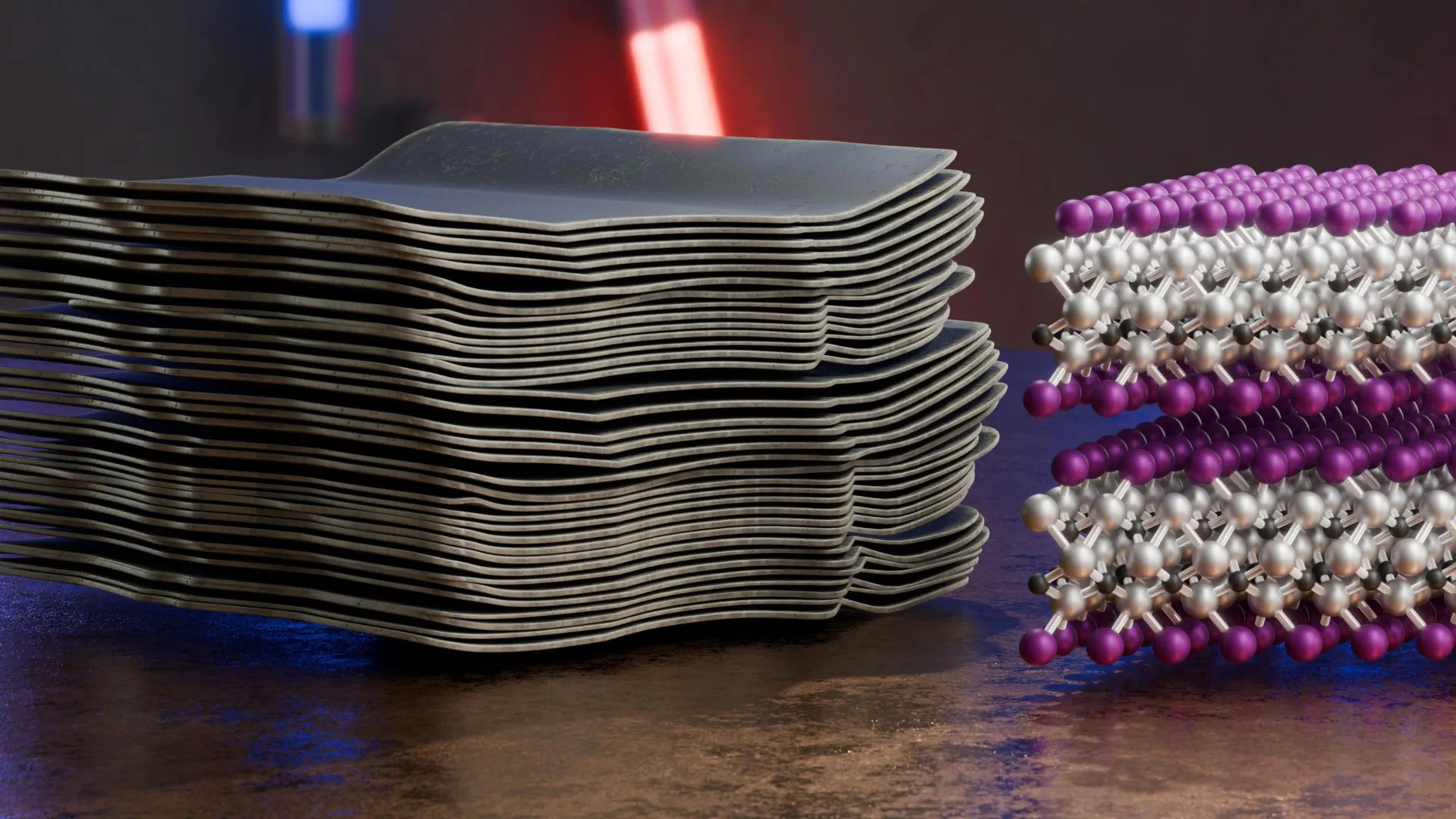
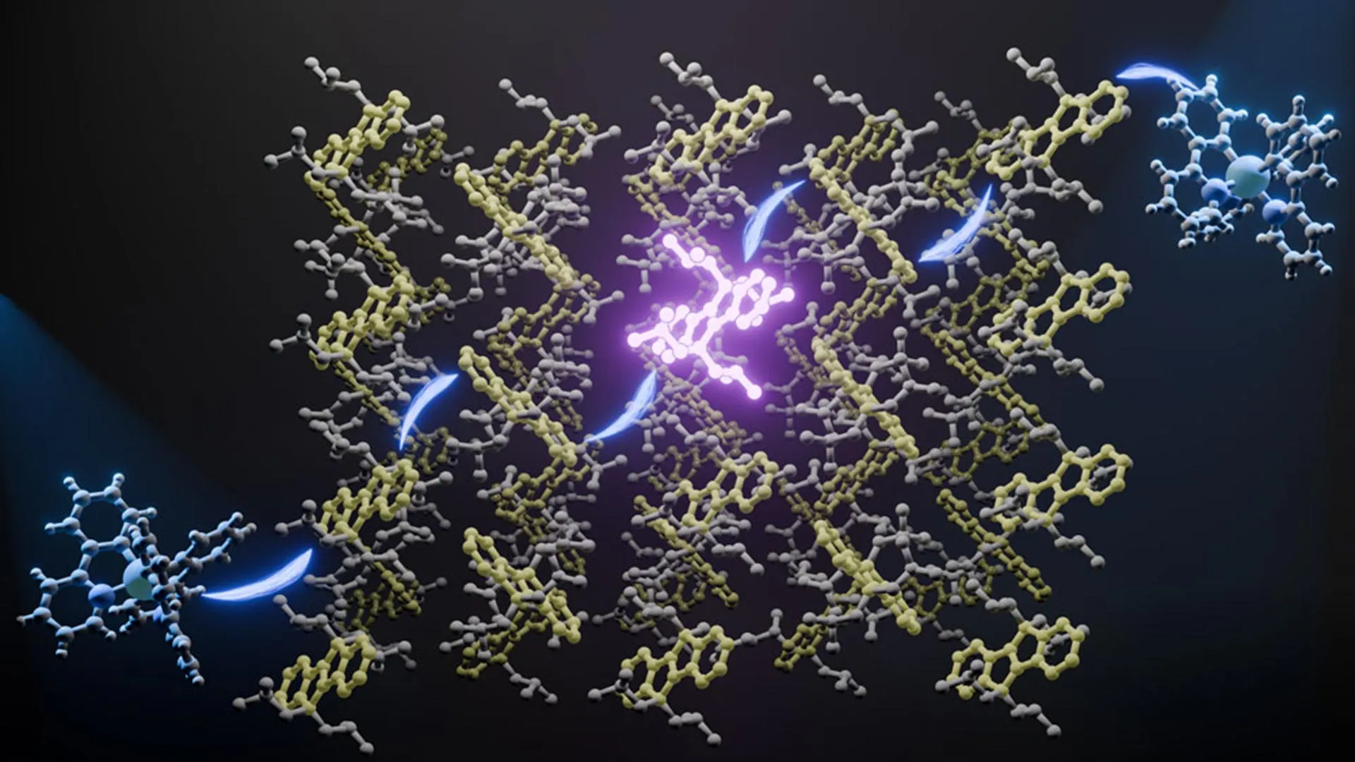
Discovered in 2011 by researchers at Drexel University, MXenes are a rapidly expanding family of two-dimensional transition metal carbides, nitrides, and carbonitrides. They are typically derived from a bulk precursor known as a MAX phase, where ‘M’ represents a transition metal (such as titanium or vanadium), ‘A’ is an element from the main group (often aluminum or silicon), and ‘X’ is carbon or nitrogen. By selectively removing the ‘A’ layer, scientists create stacked, ultra-thin sheets that possess a unique combination of metallic conductivity and hydrophilic (water-attracting) properties.
However, the "A" layer cannot simply be peeled away; it must be dissolved. For the past thirteen years, the industry standard for this process has been wet chemical etching, often involving hydrofluoric acid or similar harsh reagents. While effective at creating the 2D structure, this process leaves the outer surfaces of the MXenes covered in a random "soup" of atoms, such as oxygen (-O), hydroxyl (-OH), fluorine (-F), or chlorine (-Cl).
In the world of nano-electronics, these surface atoms are not merely passive spectators. As Dr. Mahdi Ghorbani-Asl from HZDR explains, they are the primary architects of the material’s behavior. These atoms influence how electrons move through the lattice, how the material interacts with light and heat, and how stable it remains in various chemical environments. The inherent disorder of traditional etching has long been the "Achilles’ heel" of MXenes, creating what Dr. Dongqi Li of TU Dresden describes as atomic "potholes" that scatter electrons and hinder the material’s theoretical performance limits.
The GLS Method: A Paradigm Shift in Synthesis
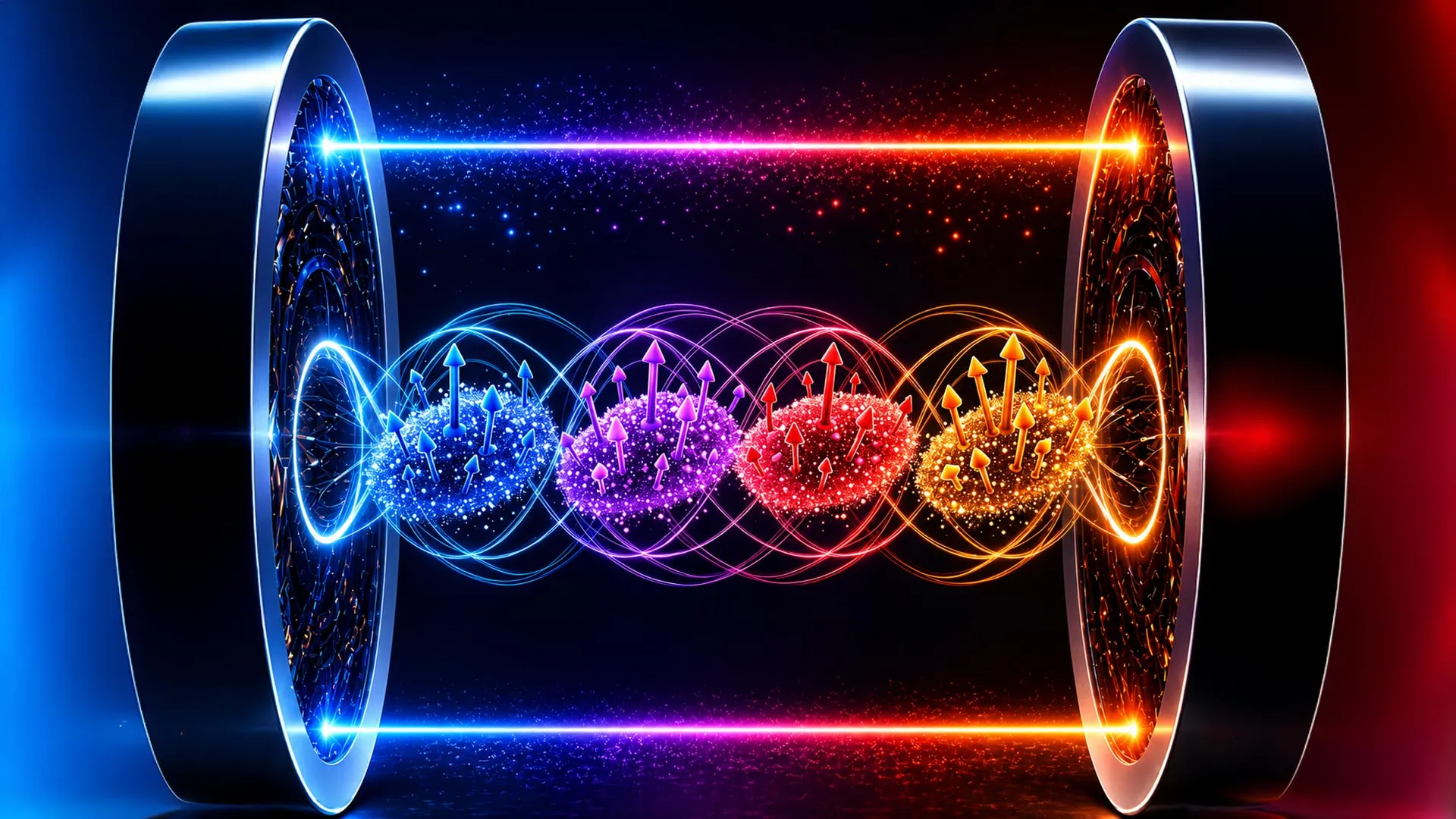
The newly developed GLS method sidesteps the limitations of wet chemistry by utilizing a high-temperature, controlled environment. Instead of acidic solutions, the process begins with solid MAX phases placed in a reaction chamber with molten salts and iodine vapor. This gaseous and liquid environment allows for a far more surgical removal of the intervening layers and, crucially, provides a controlled pathway for specific halogen atoms to bond with the transition metal surfaces.
By fine-tuning the chemical environment during the reaction, the research team demonstrated the ability to choose which halogen—chlorine, bromine, or iodine—attaches to the MXene surface. This level of precision ensures that the resulting surface atoms are arranged in a uniform, highly ordered crystalline structure. This lack of "atomic clutter" results in a significantly cleaner material with drastically reduced impurities, allowing the intrinsic properties of the transition metal core to shine through.
The versatility of the GLS method was proven through the successful production of MXenes from eight distinct MAX phases. This suggests that the technique is not a niche solution for a single material but a broad platform capable of generating a wide library of high-quality 2D materials.
Quantitative Analysis: Breaking Conductivity Records
To measure the real-world impact of this structural order, the research team focused on titanium carbide (Ti3C2), the most widely studied member of the MXene family. In conventional Ti3C2, the surface is typically a messy mixture of oxygen and chlorine, leading to significant electron scattering. Using the GLS method, the team synthesized Ti3C2Cl2—a variant where only chlorine atoms are present in a perfectly ordered arrangement.
The experimental data revealed improvements that exceeded theoretical expectations:
- Macroscopic Conductivity: The chlorine-terminated MXene exhibited a 160-fold increase in macroscopic conductivity compared to its chemically etched counterparts. This allows for much more efficient power transmission in micro-circuits.
- Terahertz (THz) Conductivity: In the high-frequency range, which is critical for the future of 6G telecommunications and high-speed data processing, the material showed a 13-fold enhancement.
- Charge Carrier Mobility: A critical metric for semiconductor performance, the mobility of electrons—how freely they move through the material—increased by nearly 400%.
These gains are attributed to the "smoothing" of the electronic landscape. When surface atoms are ordered, the quantum mechanical "traps" that normally snag electrons are eliminated. This was further confirmed through quantum transport simulations and density functional theory (DFT) calculations, which provided a microscopic view of how the ordered chlorine atoms minimize scattering.
Chronology of MXene Development and the Path to the GLS Breakthrough
The journey to this discovery has been marked by several key phases in material science:
- 2011: The first MXene, Ti3C2, is discovered at Drexel University, sparking a global interest in 2D materials beyond graphene.
- 2012–2016: Research focuses on the energy storage potential of MXenes, particularly for supercapacitors and batteries, due to their high surface area and conductivity.
- 2017–2020: Scientists identify the "surface termination problem," noting that the random distribution of -O, -F, and -OH groups limits the reproducibility of electronic devices.
- 2021: Early experiments with molten salt synthesis begin to show promise in creating halogen-terminated MXenes, but precision control remains elusive.
- 2023–2024: The HZDR and TU Dresden team perfects the GLS method, integrating iodine vapor to achieve the first truly ordered, high-purity halogenated surfaces.
Implications for Future Technology: Beyond Conductivity
The ability to "tune" the surface of an MXene does more than just improve electricity flow; it allows scientists to engineer how the material interacts with the electromagnetic spectrum. The study found that by swapping chlorine for bromine or iodine, the frequency at which the material absorbs electromagnetic waves shifts predictably.
- Electromagnetic Shielding and Stealth: Chlorine-terminated MXenes show intense absorption in the 14-18 GHz range (Ku-band), which is vital for satellite communications and radar. By adjusting the surface halogen, coatings could be designed to absorb specific radar frequencies, making them invaluable for aerospace and defense applications.
- Advanced Wireless Systems: The massive boost in THz conductivity positions these MXenes as leading candidates for 6G antennas and components, where traditional materials struggle with signal loss and heat generation.
- Catalysis and Energy: The ordered surfaces provide a more predictable environment for chemical reactions. This could lead to more efficient hydrogen production (water splitting) or improved CO2 capture technologies.
- Optoelectronics: Because the surface atoms dictate how the material interacts with light, ordered MXenes could be used to create ultra-thin, flexible sensors and displays with higher clarity and lower power consumption.
Analysis of Global Impact and Industry Reaction
While the research community has reacted with enthusiasm, industry analysts suggest that the GLS method’s primary hurdle will be scaling. Traditional chemical etching, while messy, is relatively easy to perform at scale in liquid baths. The GLS method requires high-temperature furnaces and vacuum-controlled environments. However, the sheer magnitude of the performance increase—the 160-fold conductivity boost—is likely to outweigh the initial infrastructure costs for high-end applications like semiconductor manufacturing and aerospace.
"By combining theory with our experimental ability to precisely control surface terminations, we open a new path toward MXenes with improved stability and tailored functional properties," noted Dr. Ghorbani-Asl. This sentiment highlights a growing trend in "materials by design," where researchers no longer accept the accidental properties of a substance but instead engineer them atom-by-atom.
The potential to create "hybrid" surfaces—where researchers can mix two or three different halogens in specific ratios—further expands the toolkit. This level of customization is unprecedented in 2D materials and could lead to a new class of "smart" materials that react to environmental changes by altering their electronic state.
Conclusion: A New Standard for 2D Materials
The work conducted at the Institute of Ion Beam Physics and Materials Research at HZDR and TU Dresden marks a definitive end to the "pothole" era of MXene research. By proving that surface order is the key to unlocking the true potential of these materials, the team has provided a blueprint for the next generation of electronic and optoelectronic devices.
As the industry moves toward faster, smaller, and more efficient technology, the ability to control matter at the atomic level becomes the ultimate competitive advantage. The GLS method does not just provide a cleaner material; it provides a more predictable and powerful foundation for the future of nanotechnology. With the path now cleared for improved stability and functional tailoring, MXenes are poised to move from laboratory curiosities to the backbone of 21st-century infrastructure.


Leave a Reply