
In a breakthrough that could redefine the trajectory of global computing and telecommunications, a multidisciplinary team of scientists at Monash University has successfully engineered a miniaturized photonic circuit capable of generating, routing, and reading information carried by light within a single, integrated chip. This development represents a pivotal advancement in the field of "valleytronics," an emerging branch of condensed-matter physics that utilizes the "valley degree of freedom" in electrons to encode and process data. By successfully housing these complex operations on a single platform, the researchers have addressed a decade-long challenge in the transition from theoretical quantum physics to practical, scalable technology.
The research, led by the Monash School of Physics and Astronomy and published in the prestigious journal Nature Photonics, describes a system that merges advanced nanotechnology with ultra-thin, two-dimensional materials. This integrated approach allows for the manipulation of light signals at the nanoscale, offering a blueprint for future computing systems that are significantly faster and more energy-efficient than current silicon-based electronics. As the global demand for data processing continues to outpace the physical limits of traditional semiconductors, this "all-in-one" photonic solution provides a viable path toward the next generation of high-performance hardware.
The Science of Valleytronics: A New Paradigm in Information Processing
To understand the magnitude of the Monash discovery, it is necessary to examine the limitations of modern electronics. For decades, computers have relied on "spintronics" or traditional charge-based electronics, where information is processed by moving electrons or utilizing their spin. However, as transistors shrink to the atomic scale, they generate excessive heat and encounter quantum tunneling issues, leading to a plateau in processing speeds known as the "end of Moore’s Law."
Valleytronics offers a sophisticated alternative. In certain crystalline materials, electrons possess multiple energy minima known as "valleys." These valleys can be used to store and transmit information, much like the "0" and "1" in classical computing or the "up" and "down" states in spintronics. By manipulating which valley an electron occupies—a property referred to as the valley degree of freedom—scientists can encode data with high density and minimal energy loss.
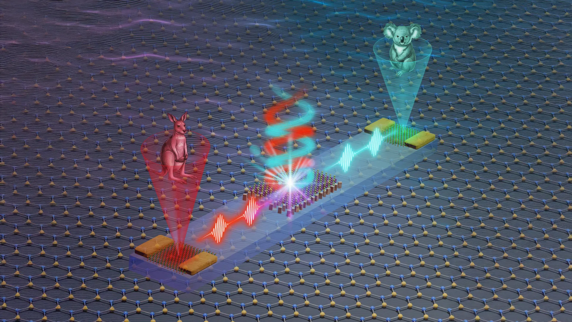
While the potential of valleytronics has been recognized for years, the primary obstacle has been the lack of an integrated system. Previous experiments required bulky, external laboratory equipment to either generate the valley signals or detect them. The Monash team’s achievement lies in the successful "on-chip" integration of the entire lifecycle of a valleytronic signal: its creation, its precise navigation through a circuit, and its final conversion into an electrical signal that a computer can understand.
Architectural Innovation: Metasurfaces and Atomic-Scale Materials
The technical core of the new device involves a sophisticated interplay between two-dimensional materials and engineered nanostructures. The team utilized ultra-thin materials, often only a few atoms thick, known as transition metal dichalcogenides (TMDCs). These materials are prized in quantum research for their unique ability to interact with light and maintain valley-specific properties.
However, 2D materials alone are difficult to control. To solve this, the Monash researchers paired these materials with "metasurfaces"—specially engineered surfaces covered in sub-wavelength structures that can bend and steer light in ways that natural materials cannot.
"We employ a straightforward stacking approach to integrate ultra-thin materials with metasurfaces," explained Dr. Kaijian Xing, co-first author of the study and a Research Fellow at Monash University. "This method overcomes the significant technical hurdles associated with direct material growth on photonic structures. By stacking these layers, we have created a modular and highly effective platform that can be scaled for further advances in valleytronics."
This "stacking" technique is a departure from traditional semiconductor fabrication, allowing for greater flexibility in design. The metasurfaces act as the "traffic controllers" for the light-encoded information, ensuring that signals are directed to specific parts of the chip with high precision, avoiding the interference and signal degradation that have plagued previous attempts at integrated valleytronics.
Overcoming the Temperature Barrier
Perhaps the most commercially significant aspect of the Monash chip is its ability to operate at room temperature. A major bottleneck for most quantum-based technologies—including many forms of quantum computing and advanced superconductivity—is the requirement for cryogenic cooling. Systems that only function at temperatures near absolute zero are expensive, energy-intensive, and physically cumbersome, limiting their use to specialized laboratories.
By demonstrating that valley-polarized light signals can be managed on an integrated chip at ambient temperatures, the Monash team has moved the technology from the realm of fundamental science into the sphere of practical engineering. This makes the technology compatible with existing infrastructure and opens the door for its eventual integration into consumer electronics, data centers, and mobile devices.
Experimental Success: Processing Parallel Data Streams
To prove the functional utility of the chip, the researchers conducted an experiment involving the simultaneous processing of multiple data streams. In a demonstration of the device’s high-fidelity routing capabilities, the team successfully encoded and processed two separate images at the same time through the same chip.
This experiment highlighted the "massive bandwidth" potential of photonic systems. Unlike traditional electrical circuits, where signals can interfere with one another if placed too closely, light-based signals can be multiplexed—sent simultaneously through the same medium—without loss of integrity. The ability to handle multiple streams of information with high precision suggests that valleytronic chips could lead to a dramatic increase in the throughput of data centers and telecommunications networks.
A Global Collaborative Effort
The development of the integrated valleytronics chip was not an isolated event but the result of an extensive international collaboration. The project brought together leading experts from Australia, China, Singapore, Germany, and Japan. This cross-border synergy combined expertise in nanophotonics, optoelectronics, and materials science.
The Monash University team, which included Dr. Chi Li, Dr. Kaijian Xing, Professor Michael S. Fuhrer, Professor Stefan A. Maier, and Dr. Haoran Ren, worked alongside contributors from the Singapore University of Technology and Design, LMU Munich, and the University of Technology Sydney. This level of collaboration underscores the global importance of finding a successor to current silicon-based technologies.
Professor Stefan A. Maier, Head of the School of Physics and Astronomy at Monash, emphasized the bridge this research builds between theory and application. "This is an important step toward fully integrated valleytronic systems," Maier said. "By combining light and quantum materials on a chip, we can access new ways of encoding and processing information that were previously theoretical."
Implications for Industry and the Environment
The implications of this breakthrough extend far beyond the laboratory. As the world moves toward an increasingly digital economy, the energy consumption of data processing has become a major environmental concern. Data centers currently account for a significant percentage of global electricity usage, much of which is spent on cooling systems to manage the heat generated by traditional electronic chips.
Photonic and valleytronic systems generate significantly less heat because they rely on light (photons) rather than the movement of electrons through resistive materials. By reducing the energy required for data transmission and processing, the Monash technology could contribute to more sustainable IT infrastructure.
Furthermore, the technology holds immense promise for:
- Quantum Computing: Providing a stable, room-temperature platform for quantum bits (qubits) based on valley states.
- Secure Communications: Leveraging the quantum properties of light for unhackable data transmission through quantum cryptography.
- Advanced Imaging: Enabling ultra-fast sensors and imaging devices for medical and industrial use.
- Optical Telecommunications: Expanding the bandwidth of fiber-optic networks by integrating processing power directly into the photonic layer.
Future Outlook: Toward Scalable Production
While the Monash chip is a landmark achievement, the researchers are already looking toward the next phase of development. The current challenge lies in scaling the fabrication process. While the "stacking" method is effective for creating high-performance prototypes, industry-wide adoption will require the development of automated, large-scale manufacturing techniques compatible with existing foundry processes.
Dr. Haoran Ren, leader of the Monash NanoMeta Group, believes the path forward is clear. "This is a significant step toward scalable, chip-based technologies that use light instead of electricity to process information," Ren stated. "What we have achieved has strong potential for applications in quantum computing and next-generation optical communication systems."
As the semiconductor industry searches for a "Post-Silicon" era solution, the Monash University integrated valleytronics chip stands out as a frontrunner. By solving the integration problem and demonstrating room-temperature stability, the team has provided a tangible glimpse into a future where the speed of light is the only limit to our computing power.
The research was supported by the Australian Research Council (ARC) and various international funding bodies, highlighting the strategic priority placed on quantum material research by global governments. With the foundational "all-in-one" chip now a reality, the race to bring valleytronics to the commercial market has officially entered a new, more accelerated chapter.


Leave a Reply