

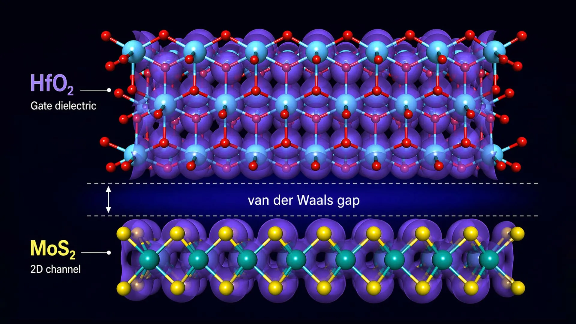
The global semiconductor industry stands at a critical juncture as traditional silicon-based transistors approach their absolute physical limits. For years, the scientific community has heralded two-dimensional (2D) materials, such as graphene and molybdenum disulfide, as the successors to silicon, promising a new era of ultra-miniaturized, high-performance electronics. However, a groundbreaking study from the Institute for Microelectronics at TU Wien (Vienna) has identified a fundamental physical barrier that could derail these ambitions. Researchers have discovered that an unavoidable atomic-scale gap, measuring a mere 0.14 nanometers, forms between 2D materials and their essential insulating layers. This "van der Waals gap," while seemingly infinitesimal, creates a significant drop in capacitive coupling, potentially rendering many 2D materials ineffective for practical integration into future computer chips.
The findings, led by Professor Mahdi Pourfath and Professor Tibor Grasser, suggest that the current trajectory of 2D material research may be overlooking a critical interface problem. As the industry prepares to invest billions of dollars into sub-2-nanometer process nodes, this revelation serves as a stark warning: without a radical redesign of how these materials are bonded, the transition to 2D electronics may hit a functional dead end before it even begins.
The Crisis of Miniaturization and the Rise of 2D Materials
For over half a century, the semiconductor industry has been governed by Moore’s Law—the observation that the number of transistors on a microchip doubles approximately every two years. This progress has been achieved primarily through "scaling," the process of shrinking individual components to fit more onto a single piece of silicon. However, as transistors shrink toward the 3-nanometer and 2-nanometer scales, silicon begins to lose its effectiveness. At these dimensions, quantum tunneling and heat dissipation become insurmountable obstacles, leading researchers to seek alternative materials.
Enter 2D materials. Unlike bulk silicon, these substances consist of a single layer of atoms or just a few atomic layers. Graphene, discovered in 2004, was the first to capture global attention due to its extraordinary electrical conductivity. It was soon followed by a class of materials known as Transition Metal Dichalcogenides (TMDs), such as molybdenum disulfide (MoS2). These materials are prized because they remain stable even when they are only three atoms thick, offering the potential for transistors that are significantly smaller and more energy-efficient than anything currently possible with silicon.
The "International Roadmap for Devices and Systems" (IRDS) has long identified 2D materials as a key pillar for the post-silicon era. Major industry players, including TSMC, Intel, and Samsung, have established dedicated research divisions to explore the integration of these "flat" materials into their manufacturing pipelines. However, the TU Wien study highlights that the focus may have been too narrow, centering on the properties of the 2D materials themselves while neglecting the complex interfaces required to make them function within a device.
The Mechanics of the Interface: Understanding the 0.14-Nanometer Barrier
A transistor does not consist of a semiconductor alone. To function as a switch, it requires a gate electrode to control the flow of current. This electrode must be separated from the semiconductor by an insulating layer, typically a high-k dielectric oxide. In conventional silicon chips, these layers are chemically bonded, creating a seamless transition that allows for efficient electrostatic control.
The research conducted by Pourfath and Grasser reveals that this seamless transition is absent in most 2D material configurations. Because 2D materials have "satisfied" chemical bonds on their surfaces, they do not easily form strong covalent bonds with the insulating oxides placed on top of them. Instead, they are held together by van der Waals forces—the same weak electromagnetic attractions that allow geckos to climb walls.
"In many combinations of 2D materials and insulating layers, the bonding between them is relatively weak," explains Professor Tibor Grasser. "As a result, the two layers do not come into close contact—there is always a gap between them."
This gap, while measuring only 0.14 nanometers, is a significant distance at the atomic scale. To provide a sense of scale, a single sulfur atom is larger than this gap, and a SARS-CoV-2 virus is approximately 700 times larger. Despite its small size, the gap acts as an additional, unwanted insulating layer with a very low dielectric constant. This weakens the "capacitive coupling"—the ability of the gate electrode to influence the semiconductor. When the coupling is weak, the transistor requires more voltage to switch, generates more heat, and fails to achieve the high speeds required for modern computing.
Chronology of 2D Semiconductor Development
The journey toward 2D electronics has been marked by several key milestones, but also by a growing realization of the challenges involved in mass production:
- 2004: Andre Geim and Konstantin Novoselov at the University of Manchester isolate graphene using the "Scotch tape method," winning the Nobel Prize in Physics six years later.
- 2011: Researchers at EPFL in Switzerland demonstrate the first functional transistor made from molybdenum disulfide (MoS2), proving that 2D materials other than graphene (which lacks a bandgap) could be used for logic circuits.
- 2016-2018: The semiconductor industry begins incorporating 2D materials into official roadmaps. Research shifts from basic physics to "integration," focusing on how to grow these materials on 300mm silicon wafers.
- 2021: TSMC and MIT announce a breakthrough in using semi-metal bismuth as a contact material to reduce resistance in 2D devices, a major step toward commercialization.
- 2023-2024: The focus shifts toward the dielectric interface. Research teams worldwide begin to report "mobility degradation" in 2D devices that cannot be explained by the material’s purity alone.
- Present: The TU Wien study identifies the van der Waals gap as the fundamental physical culprit behind these performance issues, challenging the feasibility of current integration methods.
Data and Comparative Metrics: The Hidden Cost of the Gap
To quantify the impact of the 0.14nm gap, the TU Wien team utilized advanced computational models to simulate the performance of 2D transistors. Their data suggests that the presence of the gap can reduce the effective capacitance of the gate by as much as 30% to 50% in certain configurations.
In the world of semiconductor manufacturing, where a 5% improvement in performance is considered a generational leap, a 30% loss due to an unavoidable physical gap is catastrophic. This loss effectively cancels out the benefits gained by using a 2D semiconductor in the first place.
Furthermore, the research indicates that as the insulating layer is made thinner to facilitate miniaturization, the relative impact of the van der Waals gap increases. In a transistor where the insulator is only 1 or 2 nanometers thick, a 0.14nm gap represents a substantial portion of the total stack, creating a "floor" for how thin the effective oxide thickness (EOT) can ever become.
The Economic Imperative: Billions of Dollars at Stake
The semiconductor industry is currently in the midst of a massive capital expenditure cycle. The U.S. CHIPS and Science Act, along with similar initiatives in the European Union and China, has earmarked hundreds of billions of dollars for the development of next-generation chip technology. A significant portion of this R&D funding is directed toward finding a "beyond-silicon" solution.
The TU Wien findings suggest that a portion of this investment may be at risk. If the industry continues to develop 2D materials using traditional oxide deposition methods (such as Atomic Layer Deposition or ALD), they may find that the resulting chips are no faster or more efficient than the silicon-based FinFET or Gate-All-Around (GAA) transistors they are meant to replace.
"Our work is good news for the semiconductor industry in the long run," says Grasser. "We can predict which materials are suitable for future miniaturization steps—and which are not. But if one focuses only on the 2D materials themselves, without considering the unavoidable insulating layers from the outset, there is a risk of investing billions in an approach that simply cannot succeed for fundamental physical reasons."
Strategic Solutions: The Rise of "Zipper Materials"
Despite the sobering nature of the discovery, the TU Wien researchers have proposed a path forward. The solution lies in moving away from materials that merely sit on top of one another and toward what they call "zipper materials."
Zipper materials are combinations of semiconductors and insulators that are designed to interlock at the atomic level. Instead of relying on weak van der Waals forces, these materials form strong chemical or structural bonds that effectively "zip" the two layers together, eliminating the 0.14nm gap.
This approach requires a paradigm shift in materials science. Rather than picking a 2D material for its electrical properties and then trying to find a compatible insulator, engineers must design the two layers as a single, integrated system from the start. Some promising candidates include hexagonal boron nitride (hBN) used in conjunction with specific 2D semiconductors, or the development of native oxides that can be grown directly from the 2D layer itself, ensuring a seamless interface.
Expert Analysis and Industry Impact
Industry analysts suggest that the TU Wien study will likely trigger a re-evaluation of current R&D roadmaps at major foundries. While the 2-nanometer node (expected around 2025) will likely still rely on silicon-based GAA technology, the 1-nanometer node and beyond are where 2D materials were expected to take center stage.
The discovery of the van der Waals gap adds a new layer of complexity to the "Red Brick Wall"—a term used in the industry to describe the point at which known physical laws prevent further scaling. To climb this wall, the industry must now solve a three-dimensional problem in a two-dimensional space: how to maintain the thinness of the material while ensuring the structural integrity and electrical coupling of the interface.
Furthermore, this research underscores the importance of academic-industry collaboration. The Institute for Microelectronics at TU Wien has a long history of providing the theoretical and simulation frameworks that the industry uses to validate new designs. By identifying this "fundamental physical barrier" now, they provide the industry with the lead time necessary to pivot toward zipper materials or other alternative architectures.
Conclusion: A New Design Philosophy for the Sub-1nm Era
The transition from bulk materials to atomic-scale layers is perhaps the greatest challenge in the history of electronics. As the TU Wien research demonstrates, the rules of physics change when materials are stripped down to their basic atomic components. The discovery of the 0.14-nanometer van der Waals gap serves as a reminder that in the world of nanotechnology, the spaces between things are often just as important as the things themselves.
The semiconductor industry is no stranger to overcoming "impossible" barriers. From the introduction of copper interconnects to the development of Extreme Ultraviolet (EUV) lithography, engineers have consistently found ways to push the boundaries of the possible. The challenge now is to move beyond the fascination with 2D materials as isolated wonders and embrace the complex reality of the interfaces that bind them. By focusing on "zipper materials" and integrated design, the industry may yet realize the promise of 2D electronics, ensuring that the march of technological progress continues into the sub-nanometer realm.



















Leave a Reply