
The pursuit of next-generation wearable electronics, ranging from augmented reality (AR) glasses that look like standard spectacles to sophisticated smart contact lenses, has long been stymied by the physical limitations of traditional optics. Conventional lenses, made of glass or plastic, rely on their curved geometry to bend and focus light, a process that necessitates a certain degree of bulk and thickness. However, a groundbreaking international study has identified a natural material capable of manipulating light at the atomic level, potentially rendering bulky hardware obsolete. A collaborative research team, led by the deep-tech company XPANCEO alongside scientists from the National University of Singapore and the University of Chemistry and Technology, Prague, has successfully mapped the optical constants of molybdenum oxychloride (MoOCl2), a layered crystal that exhibits the strongest light-bending effect ever recorded in a natural substance.
This discovery, recently detailed in the journal Nano Letters, represents a fundamental shift in nanophotonics. By providing the first comprehensive experimental mapping of the crystal’s optical behavior, the researchers have moved beyond theoretical observation into the realm of practical engineering. The findings suggest that MoOCl2 could serve as the foundational material for optical components that are thousands of times thinner than a human hair, yet significantly more powerful than the components currently found in high-end cameras and fiber-optic systems.
The Evolution of 2D Materials in Modern Optical Engineering
The research into MoOCl2 sits at the intersection of two rapidly evolving fields: two-dimensional (2D) materials and nanophotonics. Since the isolation of graphene in 2004, scientists have been searching for other layered materials that possess unique electronic and optical properties. While graphene is prized for its conductivity, and transition metal dichalcogenides (TMDs) are studied for their semiconducting properties, MoOCl2 has emerged as a frontrunner for specialized light manipulation.
The necessity for such materials arises from the "miniaturization wall" faced by the tech industry. As devices like smartphones and laptops shrink, the optical components—lasers, sensors, and lenses—have remained relatively large because they are governed by the laws of classical refraction. To move beyond this, engineers require materials that interact with light through quantum and atomic-scale mechanisms. The mapping of MoOCl2’s dielectric tensor provides the "blueprint" needed to build these devices, offering a level of precision that was previously unattainable.
A Chronology of Discovery: From Theory to Experimental Mapping
The path to the current breakthrough was paved by several years of incremental discoveries. Physicists first took notice of MoOCl2 due to its classification as a "bad metal," a term used to describe materials that conduct electricity but do not follow the standard rules of metallic conductivity.
In 2021 and 2022, preliminary studies published in high-impact journals like Science and Nature Communications highlighted the existence of "hyperbolic plasmon polaritons" within the crystal. These are specialized light waves that are tightly confined to the surface of the material, allowing light to be guided in specific directions without the usual scattering or diffraction. While these studies proved that the material had extraordinary potential, they were largely observational. The scientific community could see that the light was behaving strangely, but they lacked the specific numerical data—the optical constants—to explain why or to use the material in a controlled manufacturing process.
Recognizing this gap, the team from XPANCEO and their academic partners initiated a rigorous experimental campaign. They employed advanced spectroscopic techniques to measure how the material responds to different wavelengths of light across various orientations. The culmination of this effort was the publication in Nano Letters, which finally provided the complete dielectric tensor of MoOCl2, effectively turning a scientific curiosity into an engineering tool.
The Optical Chameleon: Anisotropy and the Birefringence Record
At the heart of MoOCl2’s utility is its extreme optical anisotropy. In most materials, such as glass or water, light travels at the same speed regardless of the direction it enters. In anisotropic materials, the internal structure dictates that light behaves differently depending on its path.
MoOCl2 takes this to an extreme, acting as a "chameleon." When the crystal is oriented along one axis, it behaves like a metal, reflecting light with high efficiency. However, when rotated by 90 degrees, it shifts its character entirely, becoming as transparent as glass. This occurs because of the material’s unique atomic structure, which features one-dimensional chains of molybdenum atoms. Electrons move with ease along these chains (metallic behavior) but encounter resistance when moving across them (dielectric behavior).
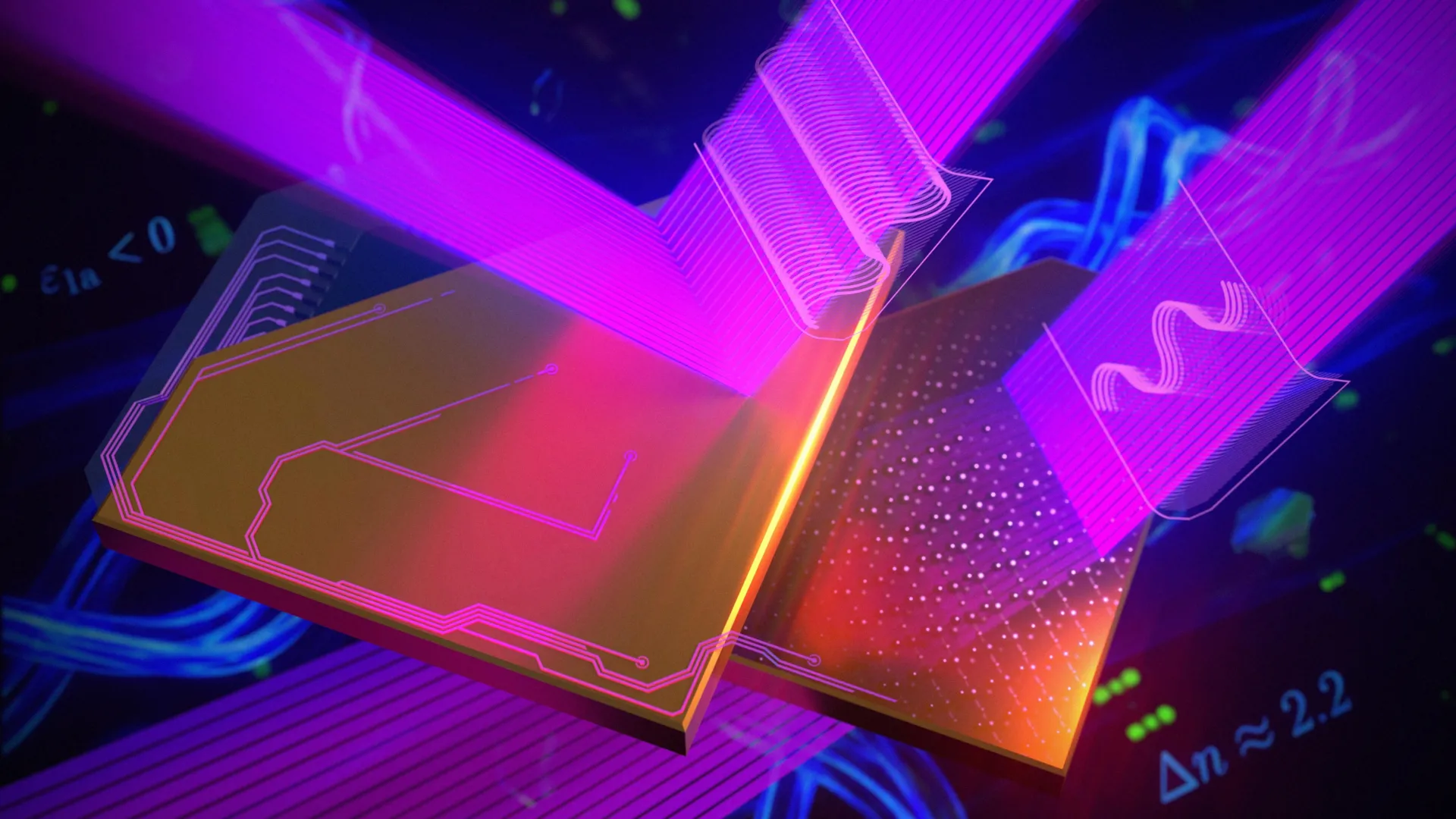
This structural arrangement results in a record-breaking in-plane birefringence value of approximately 2.2. To put this in perspective, calcite, a mineral long used in industry for its light-splitting capabilities, has a birefringence of about 0.17. The fact that MoOCl2 is more than ten times as effective as traditional materials allows for the creation of ultrathin "waveplates" and polarizers. These components are essential for AR displays, where light must be precisely polarized to create clear, overlaid digital images without adding weight to the user’s face.
Slowing Light: The Epsilon-Near-Zero Phenomenon in Visible Light
Perhaps the most significant technical finding in the study is the identification of an "epsilon-near-zero" (ENZ) point at 512 nanometers. This wavelength corresponds to green light, which is the part of the spectrum the human eye is most sensitive to.
At an ENZ point, the permittivity (or the material’s ability to resist an electric field) approaches zero. When this happens, the phase velocity of light becomes nearly infinite, but more importantly, the wavelength of light inside the material stretches, and the light effectively slows down. This "squeezing" of electromagnetic energy into a tiny volume dramatically boosts light-matter interactions.
Most materials that exhibit ENZ behavior do so in the ultraviolet or infrared ranges, making them difficult to use in consumer electronics. The discovery that MoOCl2 achieves this in the visible green spectrum is a major advantage. It means that the material can be integrated into existing technologies like CMOS sensors, standard lasers, and microscopic imaging systems. By slowing light down, engineers can create faster data processing channels in photonic chips while consuming significantly less power, as the intensified electric field reduces the energy required to trigger a response.
Expert Analysis and Official Commentary
The implications of this research extend far beyond the laboratory. Dr. Valentyn Volkov, the founder and CTO of XPANCEO and the study’s corresponding author, emphasized that the transition from observation to measurement is what will drive the next wave of innovation.
"Observing a phenomenon is the first step, but engineering requires precise numbers," Dr. Volkov stated. He noted that by providing the experimental foundation for MoOCl2’s behavior, the team has enabled designers to build around the material with "greater confidence." Volkov further highlighted that the relevance of this work spans compact polarization optics, nonlinear devices, and the long-term goal of "highly miniaturized integrated systems including smart contact lenses."
Industry analysts suggest that this breakthrough could accelerate the timeline for "true" AR. Current AR headsets are often criticized for being too heavy or having a "form factor" problem. By replacing bulky glass elements with MoOCl2-based nanophotonics, companies could theoretically produce glasses that are indistinguishable from standard eyewear.
Broader Impact on Integrated Photonics and Data Processing
Beyond wearables, the mapping of MoOCl2 has profound implications for the semiconductor and telecommunications industries. As traditional electronic chips approach their physical limits due to heat generation and signal interference, the industry is looking toward photonic chips, which use light instead of electrons to move data.
MoOCl2’s ability to function as a natural hyperbolic medium allows for "sub-diffractional" waveguides. In traditional optics, light cannot be guided through a space smaller than half its wavelength. However, MoOCl2 can guide light in paths smaller than this limit, allowing for much denser and more efficient optical circuits. This could lead to a new generation of "green" data centers that process information at the speed of light with a fraction of the current energy footprint.
Furthermore, the material’s potential in nonlinear nanophotonics is substantial. In these systems, light can be used to change the properties of the material itself, allowing for the creation of new colors of light or the switching of optical signals. This is a critical requirement for optical computing, where light must be used to perform logic operations.
Conclusion: The Path Toward Atomic-Scale Devices
The successful mapping of molybdenum oxychloride represents a pivotal moment in the transition from classical to quantum-enhanced optics. By harnessing a material that behaves as both a metal and a glass, and which possesses the unique ability to slow light in the visible spectrum, researchers have unlocked a new toolkit for the digital age.
The collaboration between XPANCEO, the National University of Singapore, and the University of Chemistry and Technology, Prague, underscores the importance of cross-border scientific efforts in solving complex engineering challenges. As the tech industry moves toward a future where technology is increasingly integrated into the human experience—becoming "invisible" through miniaturization—materials like MoOCl2 will likely be the silent engines driving that transformation. The data provided by this study ensures that the "invisible" future is now an engineering reality rather than a theoretical possibility.


Leave a Reply