
The global semiconductor industry stands at a critical crossroads as the physical limits of silicon-based microchips become increasingly apparent. For more than half a century, the relentless miniaturization of electronic components—governed by Moore’s Law—has driven the evolution of everything from smartphones to supercomputers. However, as transistors approach the atomic scale, traditional materials are beginning to fail, leading researchers to explore "2D materials" such as graphene and molybdenum disulfide as the next logical step. While these materials, which consist of only a few atomic layers, have long been hailed as the future of electronics, a groundbreaking study from TU Wien (Vienna) suggests that a previously overlooked physical phenomenon could derail these ambitions. Researchers have identified an unavoidable atomic-scale gap that forms between 2D materials and their insulating layers, creating a fundamental barrier to performance that could render billions of dollars in research and development obsolete if not addressed.
The Physical Constraints of Modern Miniaturization
To understand the significance of the TU Wien findings, one must first look at the current state of transistor technology. A transistor acts as a tiny switch, controlling the flow of electricity to represent the binary 1s and 0s of digital information. For decades, the industry relied on bulk silicon to create these switches. As devices grew smaller, the "gate" that controls the switch had to become more precise. In the current generation of chips, such as those found in high-end processors, transistors have transitioned from flat structures to three-dimensional designs known as FinFETs (Fin Field-Effect Transistors).
As the industry moves toward the 2-nanometer node and beyond, even FinFETs are reaching their limit. At these dimensions, silicon loses its effectiveness due to "short-channel effects," where electricity begins to leak even when the switch is supposed to be off. This has led the scientific community to focus on 2D materials—transition metal dichalcogenides (TMDs)—which are thin enough to allow for perfect electrostatic control. However, the research led by Prof. Mahdi Pourfath and Prof. Tibor Grasser at TU Wien’s Institute for Microelectronics reveals that the transition to 2D materials is not as simple as swapping one substance for another.
The Discovery of the Van der Waals Gap
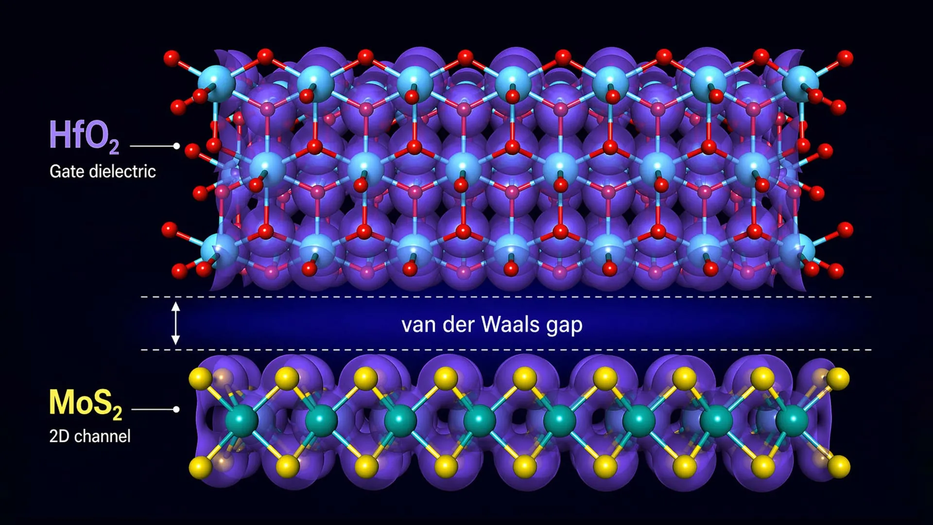
The core of the issue lies in the interface between the semiconductor and the insulator. In any transistor, the semiconductor must be separated from the gate electrode by an insulating layer, typically an oxide. This prevents a short circuit while allowing the gate to influence the semiconductor via an electric field. In traditional silicon chips, the oxide layer is chemically bonded to the silicon, creating a seamless transition.
The TU Wien team found that when 2D materials are used, this seamless transition is absent. Because 2D materials have "saturated" surfaces—meaning their atoms are already fully bonded within the layer—they do not easily form strong chemical bonds with the insulating layers placed on top of them. Instead, they are held together by van der Waals forces, which are relatively weak intermolecular attractions.
"In many combinations of 2D materials and insulating layers, the bonding between them is relatively weak," explains Prof. Tibor Grasser. "As a result, the two layers do not come into close contact—there is always a gap between them."
This gap measures approximately 0.14 nanometers. While this distance is incomprehensibly small—roughly one-seven-hundredth the size of a SARS-CoV-2 virus—it is monumental in the context of atomic-scale electronics. This "atomic gap" acts as an additional, unintended insulating layer with a very low dielectric constant. In physics terms, it weakens the capacitive coupling between the gate and the semiconductor.
The Chronology of 2D Material Research and the Current Reality Check
The journey of 2D materials in electronics began in earnest in 2004 with the isolation of graphene at the University of Manchester, a feat that earned Andre Geim and Konstantin Novoselov the Nobel Prize in Physics. Graphene’s extraordinary electron mobility sparked a global "gold rush" in materials science. However, graphene lacks a "bandgap," making it difficult to use as a transistor because it cannot be easily turned off.
By 2011, attention shifted to other 2D materials like molybdenum disulfide (MoS2), which does possess a bandgap. Over the last decade, the International Roadmap for Devices and Systems (IRDS) has identified 2D semiconductors as a primary candidate for the post-silicon era, specifically for the year 2028 and beyond.
The TU Wien study represents a "reality check" in this chronology. For years, researchers focused on the "intrinsic" properties of the materials—how fast electrons move through a pure sheet of MoS2 in a vacuum. The new research shifts the focus to the "extrinsic" reality of a finished device. It suggests that many of the performance records achieved in laboratory settings may be impossible to replicate in a mass-produced integrated circuit because the 0.14nm gap imposes a "hard ceiling" on how much a device can be miniaturized before the gate loses control over the channel.
Technical Implications: Why 0.14 Nanometers Matters
The performance of a transistor is largely determined by its Equivalent Oxide Thickness (EOT). To maintain control over the electrons in the semiconductor, the insulating layer must be as thin and "capacitive" as possible. When the 0.14nm van der Waals gap is introduced, it effectively increases the EOT.
In the race to sub-1nm EOT values required for future chip generations, a 0.14nm gap represents a massive 14% to 20% "tax" on performance. This gap reduces the "on-current" of the transistor (how much power it can deliver) and increases the "subthreshold swing" (how much voltage is required to switch the device between on and off states). For the semiconductor industry, which fights for 5% to 10% efficiency gains with each new generation, a 20% loss due to a fundamental physical gap is a catastrophic hurdle.
Industry Reactions and Economic Risks
While the semiconductor industry—led by giants such as TSMC, Intel, and Samsung—has not yet officially altered its long-term roadmaps in response to this specific study, the implications are causing ripples in the materials science community. The research serves as a warning against the "sunk cost fallacy" in scientific investment.
"Our work is good news for the semiconductor industry in the sense that it provides a roadmap for what will work," says Prof. Tibor Grasser. "But if one focuses only on the 2D materials themselves, without considering the unavoidable insulating layers from the outset, there is a risk of investing billions in an approach that simply cannot succeed for fundamental physical reasons."
Market analysts suggest that the cost of developing a new material node can exceed $5 billion for R&D alone, with the construction of a compatible fabrication plant (fab) costing upwards of $20 billion. If the "atomic gap" problem is not solved, the industry could face a massive financial loss as it reaches a dead end in 20D miniaturization.
Potential Solutions: The Rise of Zipper Materials
The TU Wien researchers are not merely identifying a problem; they are proposing a new philosophy for material design. The solution, according to Prof. Mahdi Pourfath, lies in "zipper materials."
Rather than picking a 2D semiconductor and then trying to find an insulator that fits, the two must be engineered as a single, integrated system. Zipper materials are combinations of semiconductors and insulators that form strong chemical bonds across their interface, effectively "zipping" the two layers together and eliminating the van der Waals gap.
This approach requires moving away from the "pick and place" method of stacking 2D materials. Instead, researchers are looking into epitaxial growth, where the insulating layer is grown directly onto the 2D material in a way that encourages atomic bonding. This could involve using specific dielectrics that have a high affinity for the chalcogen atoms in the 2D semiconductor, creating a seamless electronic transition.
Analysis: The Shift from Material-Centric to Interface-Centric Design
The broader impact of this research is a paradigm shift in how we approach nanotechnology. For the past two decades, the focus has been on the "hero material"—the search for a single substance that would replace silicon. The TU Wien findings suggest that the "hero" does not exist in isolation.
The future of the semiconductor industry will likely be defined not by the materials we use, but by the interfaces between them. This mirrors previous transitions in the industry. For example, in the late 1990s, the industry hit a wall with silicon dioxide insulators. The solution wasn’t just a better version of silicon; it was the introduction of high-k dielectrics and metal gates, a transition that required a total rethink of the transistor’s interface.
Conclusion and Future Outlook
The findings from TU Wien provide a sobering but necessary correction to the hype surrounding 2D materials. By highlighting the 0.14nm van der Waals gap, the research underscores that in the world of the very small, there is no such thing as a negligible distance.
As the semiconductor industry prepares for the transition to 2D electronics in the late 2020s and early 2030s, the focus must now shift to the chemistry of the interface. The "atomic gap" is a formidable barrier, but it also serves as a guidepost. By identifying the physical limitations of current approaches, scientists can now pivot toward "zipper materials" and other integrated designs that could truly deliver the next generation of ultra-powerful, ultra-efficient computing.
The stakes are high. As artificial intelligence, autonomous systems, and global data needs continue to grow, the demand for more powerful chips is insatiable. The industry’s ability to navigate the "atomic gap" will determine whether the next decade is defined by a technological plateau or a new era of unprecedented innovation. For now, the message to researchers and investors alike is clear: the material is only half the story; the interface is where the future of computing will be won or lost.


Leave a Reply