

The global semiconductor industry stands at a critical crossroads as the physical limits of silicon-based microelectronics become increasingly apparent. For more than five decades, the trajectory of computing power has been defined by the relentless pursuit of miniaturization, a phenomenon famously codified as Moore’s Law. However, as transistors shrink toward the atomic scale, traditional materials are beginning to fail, leading researchers to explore "beyond-silicon" alternatives. Among the most promising candidates are two-dimensional (2D) materials—substances like graphene or molybdenum disulfide that consist of only a single layer of atoms. Yet, a groundbreaking study from the Institute for Microelectronics at TU Wien (Vienna) suggests that these materials may face a fundamental physical barrier that could render billions of dollars in research and development investment obsolete unless a radical shift in design philosophy occurs.
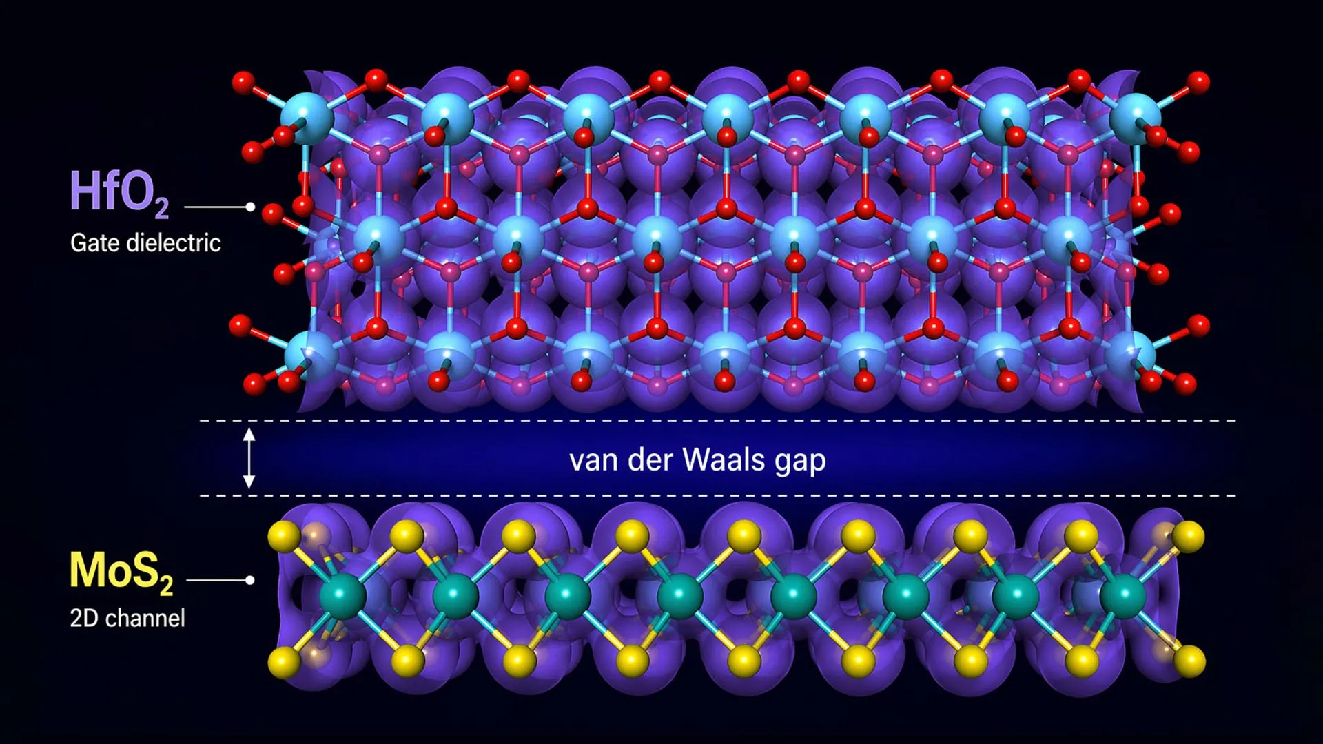
The core of the issue, as identified by Professor Tibor Grasser and Professor Mahdi Pourfath, lies not within the 2D materials themselves, but at the interface where these materials meet the insulating layers necessary for electronic function. In a modern transistor, a semiconductor is toggled between conductive and non-conductive states via a gate electrode. To ensure efficiency and prevent leakage, an insulating oxide layer must separate the gate from the semiconductor. The TU Wien team has discovered that when 2D materials are paired with these insulators, an unavoidable atomic-scale gap of approximately 0.14 nanometers forms. While seemingly negligible, this gap creates a "van der Waals" barrier that significantly degrades the electrical performance of the device, potentially halting the progress of further miniaturization.
The Evolution of Scaling: A Chronology of Semiconductor Innovation
To understand the gravity of the TU Wien findings, one must look at the historical progression of transistor technology. The journey from the first bulky vacuum tubes to the multi-billion transistor chips of today has been defined by the mastery of interfaces.
- 1947–1960: The Dawn of the Transistor. The invention of the point-contact transistor at Bell Labs replaced vacuum tubes, but early germanium-based devices were unstable. The shift to silicon occurred because silicon naturally forms a high-quality native oxide (SiO2), which serves as a near-perfect insulator.
- 1965–2000: The Golden Age of Moore’s Law. During this period, the industry focused on "dennard scaling," where reducing the size of transistors allowed for higher clock speeds and lower power consumption. The interface between silicon and its oxide remained the industry’s greatest asset.
- 2004: The Graphene Revolution. Andre Geim and Konstantin Novoselov isolated graphene, a single layer of carbon atoms, at the University of Manchester. This sparked a global race to find 2D materials that could replace silicon, as graphene’s high electron mobility promised lightning-fast processors.
- 2011–2020: The Rise of TMDs. Researchers realized that while graphene was a great conductor, it lacked a "bandgap" necessary for switching transistors off. This led to the study of Transition Metal Dichalcogenides (TMDs) like molybdenum disulfide (MoS2), which possess the semiconducting properties required for logic gates.
- 2021–Present: The Interface Bottleneck. As the industry moves toward the 2nm process node and beyond, the integration of 2D materials into existing manufacturing flows has revealed systemic issues. The TU Wien study represents a pivotal moment in this timeline, shifting the focus from material properties to interface physics.
The Physics of the 0.14-Nanometer Gap
The research conducted at TU Wien highlights a phenomenon that has been largely overlooked in the rush to celebrate the "magic" of 2D materials. In traditional silicon transistors, the atoms of the semiconductor and the insulator are chemically bonded in a robust, 3D crystalline structure. However, 2D materials are "chemically satisfied" on their surfaces, meaning they do not have "dangling bonds" to latch onto an oxide layer.
"In many combinations of 2D materials and insulating layers, the bonding between them is relatively weak," explains Professor Tibor Grasser. "They are held together only by so-called van der Waals forces. As a result, the two layers do not come into close contact—there is always a gap between them."
This gap, measuring 0.14 nanometers, is roughly half the distance between atoms in a typical solid. For comparison, the SARS-CoV-2 virus is approximately 100 nanometers in diameter, making the gap nearly 700 times smaller than a single virus particle. Despite its minuscule size, the gap acts as an additional, parasitic capacitor in series with the gate insulator. In electrical engineering terms, this increases the "Equivalent Oxide Thickness" (EOT), effectively distancing the gate electrode from the channel it is supposed to control. This loss of capacitive coupling means that more voltage is required to switch the transistor, leading to higher power consumption and heat generation—the very problems 2D materials were intended to solve.
Supporting Data: The Impact on Device Performance
The TU Wien study utilized advanced computational modeling to quantify the impact of this van der Waals gap across various material pairings. The data suggests a stark reality for the semiconductor roadmap:
- Capacitance Loss: The presence of the 0.14 nm gap can reduce the effective gate capacitance by as much as 30% to 50% in ultrathin devices. This reduction directly correlates to a slower switching speed and reduced "on-current."
- Miniaturization Limits: As the thickness of the actual insulating oxide is reduced to 1 nanometer or less (to keep up with scaling), the 0.14 nm gap becomes a dominant fraction of the total stack. At this scale, the gap represents a physical limit that cannot be overcome by simply making the oxide thinner.
- Thermal Resistance: The weak van der Waals bond also impedes heat dissipation. 2D materials are prone to overheating because phonons (vibrational energy) cannot easily cross the gap into the substrate, leading to premature device failure under high workloads.
Industry Implications and Financial Risk
The semiconductor industry is currently investing hundreds of billions of dollars into Next-Generation Lithography (EUV) and new material science. Giants such as TSMC, Intel, and Samsung are already exploring the integration of 2D channels for the "sub-1nm" era. However, the TU Wien findings serve as a warning that these investments may be misdirected if they focus solely on the quality of the 2D sheets.
"If the semiconductor industry wants to succeed with 2D materials, the active layer and the insulating layer must be designed together from the very beginning," says Professor Mahdi Pourfath.
The economic risk is significant. Developing a new fabrication process for a 2D-based chip requires retooling entire factories, a process that can cost upwards of $20 billion per facility. If the resulting chips cannot outperform silicon due to the 0.14 nm gap, the industry could face a technological "dead end" that stalls the progress of artificial intelligence, high-performance computing, and mobile technology.
The "Zipper Material" Solution
The researchers at TU Wien are not merely identifying a problem; they are proposing a path forward. The solution lies in moving away from van der Waals interfaces and toward what they term "zipper materials."
These are specific combinations of semiconductors and insulators that can form strong chemical bonds—essentially "zipping" the two layers together at the atomic level. By creating a covalent or ionic bond between the 2D material and the oxide, the 0.14 nm gap can be eliminated. This would restore capacitive coupling and allow the full potential of 2D materials to be realized.
Potential candidates for this "zipper" approach include specialized epitaxial growth techniques where the insulator is grown directly onto the 2D material in a vacuum, or the use of 2D insulators like hexagonal boron nitride (hBN) that can be stacked with high precision. However, these methods currently face challenges in large-scale industrial production, as they are far more complex than the standard deposition techniques used in today’s chip factories.
Broader Impact and the Future of Nanoelectronics
The work of the TU Wien team has prompted a re-evaluation of the International Roadmap for Devices and Systems (IRDS), the industry’s guiding document for future technology. While the discovery of the interface gap is a hurdle, Professor Grasser views it as a necessary reality check that will ultimately save the industry time and resources.
"Our work is good news for the semiconductor industry," Grasser asserts. "We can predict which materials are suitable for future miniaturization steps—and which are not. This allows us to focus our efforts on the combinations that have a fundamental physical chance of succeeding."
As the world enters an era where AI and data processing demands are skyrocketing, the need for more efficient chips has never been greater. The transition from silicon to 2D materials remains the most likely path for the 2030s, but the TU Wien research ensures that this transition will be grounded in a deeper understanding of atomic-scale physics. The "gap" may be small, but the shift in perspective it requires is massive: the future of electronics will not be determined by the materials we use, but by how well we can make them touch.



















Leave a Reply