In a landmark achievement for the field of condensed matter physics and optoelectronics, a multidisciplinary team of scientists at Monash University has announced the development of a pioneering integrated circuit capable of generating, routing, and reading information via light on a single, microscopic chip. This breakthrough, recently detailed in the prestigious journal Nature Photonics, represents a significant leap forward for "valleytronics," an emerging branch of electronics that utilizes the "valley" index of electrons or excitons to encode data. By successfully consolidating these complex functions into a unified, room-temperature system, the researchers have addressed a technical bottleneck that has hindered the transition of valley-based technologies from theoretical models to practical applications for over a decade.
The Evolution of Information Processing: Beyond Electronics and Spintronics
For more than half a century, the global computing infrastructure has relied almost exclusively on the movement of electrical charge. However, as the physical limits of silicon-based transistors are approached—a phenomenon often cited as the impending end of Moore’s Law—the scientific community has intensified its search for alternative ways to process information. While "spintronics" seeks to use the intrinsic spin of electrons, valleytronics focuses on the "valley degree of freedom."
In certain ultra-thin materials, such as transition metal dichalcogenides (TMDs), the electronic energy bands have multiple "valleys" or local minima. Electrons can occupy these different valleys, and their position serves as a binary-like state (e.g., Valley A or Valley B) that can be used to store and process information. The primary challenge has always been the volatility of these states and the difficulty of manipulating them without bulky, external laboratory equipment. The Monash University team, led by researchers from the School of Physics and Astronomy, has fundamentally altered this landscape by creating a compact, on-chip architecture that manages the entire lifecycle of a valleytronic signal.
Architectural Breakthrough: Integrating Metasurfaces and 2D Materials
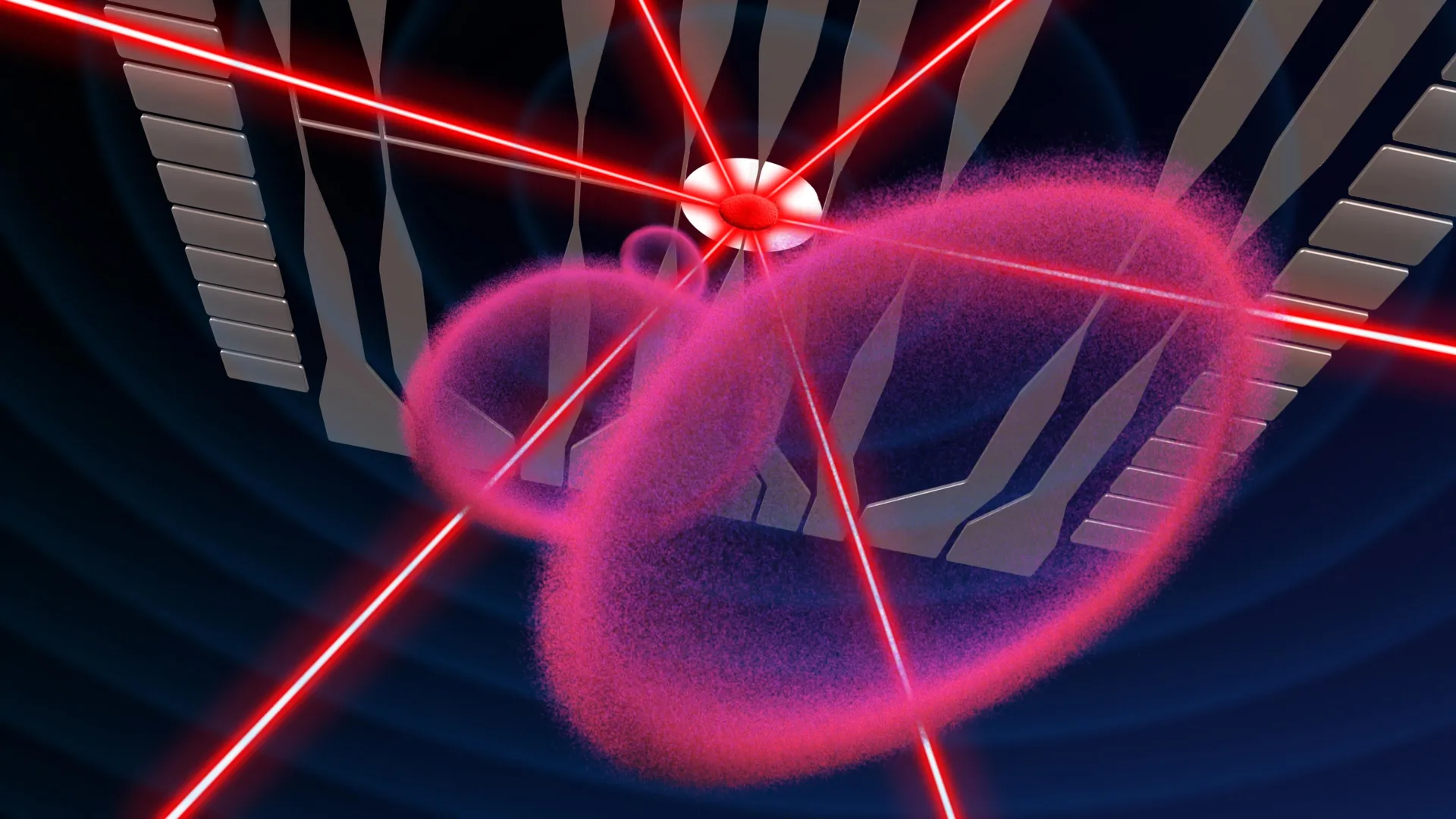
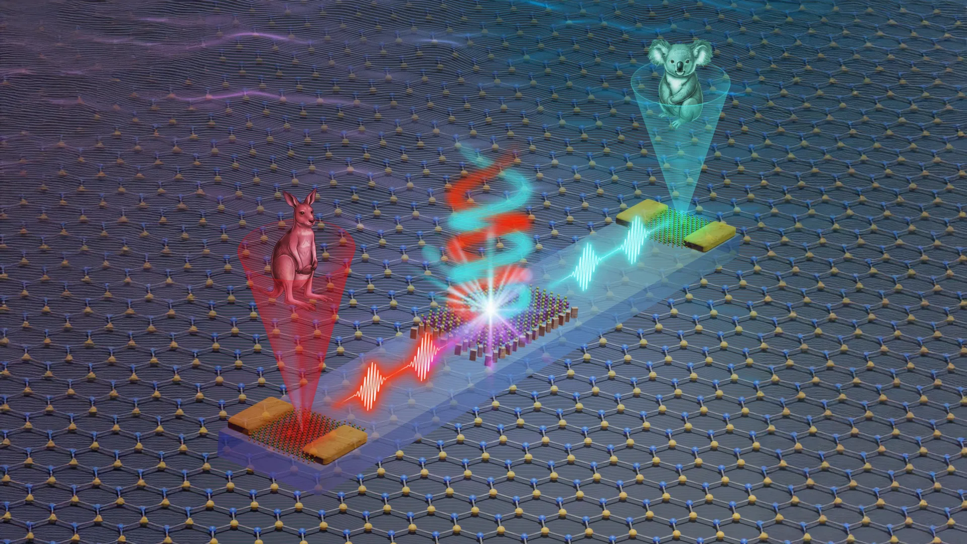
The device’s success is rooted in its sophisticated structural design, which pairs advanced nanotechnology with materials only a few atoms thick. Historically, valleytronic research faced a "fragmentation" problem: researchers could successfully generate a signal in one setup or detect it in another, but linking these processes on a single chip proved elusive due to the incompatibility of different material growth techniques.
Dr. Chi Li, the lead author of the study, emphasized that the achievement lies in the seamless integration of these components. "Until now, we could generate or detect these signals, but not do everything in one integrated device," Dr. Li noted. "What we’ve built is a complete on-chip system that can create, route, and read this information with very high precision."
To achieve this, the team employed a "straightforward stacking approach," as described by co-first author Dr. Kaijian Xing. This method allowed the researchers to place ultra-thin, two-dimensional materials directly onto engineered "metasurfaces"—nanostructured surfaces designed to interact with light in ways that natural materials cannot. By bypassing the traditional difficulties of direct material growth on photonic structures, the team ensured the integrity of the quantum properties while maintaining a scalable manufacturing logic.
The Room-Temperature Advantage
Perhaps the most commercially significant aspect of the Monash discovery is the device’s ability to operate at room temperature. A major hurdle for many quantum-based technologies, particularly those involving superconducting circuits or certain types of quantum dots, is the requirement for cryogenic cooling. Systems often need to be kept at temperatures near absolute zero (approximately -273 degrees Celsius) to prevent thermal noise from disrupting delicate quantum states.
The requirement for heavy, energy-intensive dilution refrigerators makes such technologies impractical for consumer electronics or mobile infrastructure. By achieving high-precision valleytronic control at ambient temperatures, the Monash team has opened the door for this technology to be integrated into standard data centers and eventually, perhaps, portable devices. Dr. Haoran Ren, an ARC Future Fellow and leader of the Monash NanoMeta Group, pointed out that this thermal stability is a prerequisite for any technology aiming to replace or augment current silicon-based systems.
Experimental Validation: Dual-Stream Information Processing
To demonstrate the practical utility of the chip, the researchers conducted an experiment involving the simultaneous processing of multiple data streams. In a test that simulated the demands of modern parallel computing, the chip successfully encoded and routed two separate images at the same time. This capability—multiplexing information through the valley degree of freedom—is essential for the high-bandwidth requirements of future telecommunications and AI processing.
The experiment proved that the valley degree of freedom is not just a scientific curiosity but a robust carrier of complex information. By utilizing light signals rather than electrical currents, the chip avoids the "Joule heating" that plagues traditional processors. In electrical circuits, the movement of electrons through resistive materials generates heat, which limits processing speed and wastes energy. Photonic-based valleytronics, by contrast, allows for "massive bandwidths and ultra-fast data transmission speeds" with significantly lower energy overhead.
Strategic Global Collaboration
The development of the integrated valleytronics chip was not an isolated effort but the result of an extensive international partnership. The project brought together leading minds from Australia, China, Singapore, Germany, and Japan. This collaboration combined niche expertise in several high-tech fields:
- Australia (Monash University & UTS): Led the design, fabrication, and experimental characterization.
- Singapore (SUTD): Contributed to the optimization of photonic structures.
- Germany (LMU Munich): Provided theoretical insights into light-matter interactions at the nanoscale.
- Japan & China: Assisted with material synthesis and advanced imaging techniques.
Professor Stefan A. Maier, Head of the School of Physics and Astronomy at Monash University, highlighted that this synergy was vital for bridging the gap between fundamental physics and engineering. "This is an important step toward fully integrated valleytronic systems," Professor Maier said. "By combining light and quantum materials on a chip, we can access new ways of encoding and processing information."
Broader Impact: Sustainability and the Future of Computing
The implications of this research extend far beyond the laboratory. As the world becomes increasingly reliant on Artificial Intelligence (AI) and the Internet of Things (IoT), the global demand for computing power is skyrocketing. This has led to a corresponding surge in the energy consumption of data centers, which currently account for a significant portion of global greenhouse gas emissions.
The transition to light-based, or photonic, information processing is viewed by many as a "green" computing revolution. Because light-based systems generate less heat, they require less energy for cooling—a major expense for modern tech giants. Furthermore, the high-speed nature of light allows for the processing of data at rates that electricity simply cannot match.
In the realm of security, the "valley degree of freedom" offers potential for new forms of encryption. Quantum properties are notoriously difficult to intercept or clone without detection, making valleytronic systems a candidate for the next generation of secure communication networks.
Chronology of Development and Future Outlook
The journey to this integrated chip has been a decade in the making.
- 2012–2015: Initial discovery of valley properties in monolayer TMDs (Transition Metal Dichalcogenides).
- 2016–2019: Development of metasurfaces capable of separating light based on its "handedness" or chirality, which is linked to valley states.
- 2020–2022: Breakthroughs in 2D material stacking and the realization that room-temperature operation was feasible in specific nanophotonic environments.
- 2024: The successful integration of generation, routing, and detection on a single chip, as published in Nature Photonics.
Looking ahead, the Monash team plans to refine the programmability of the chip. While the current device can route information along pre-defined paths, the next phase of research will focus on creating "reconfigurable" valleytronic circuits. Such devices would allow for the paths of light to be changed on the fly, mimicking the flexibility of software-defined networking.
Dr. Haoran Ren concluded that the work is a "significant step toward scalable, chip-based technologies." As the team looks toward commercial partnerships, the focus will shift to manufacturing scalability, ensuring that the stacking process used in the lab can be replicated in industrial semiconductor foundries. If successful, the integrated valleytronic chip may soon become a cornerstone of the next technological era, defining the transition from the age of the electron to the age of the photon.