

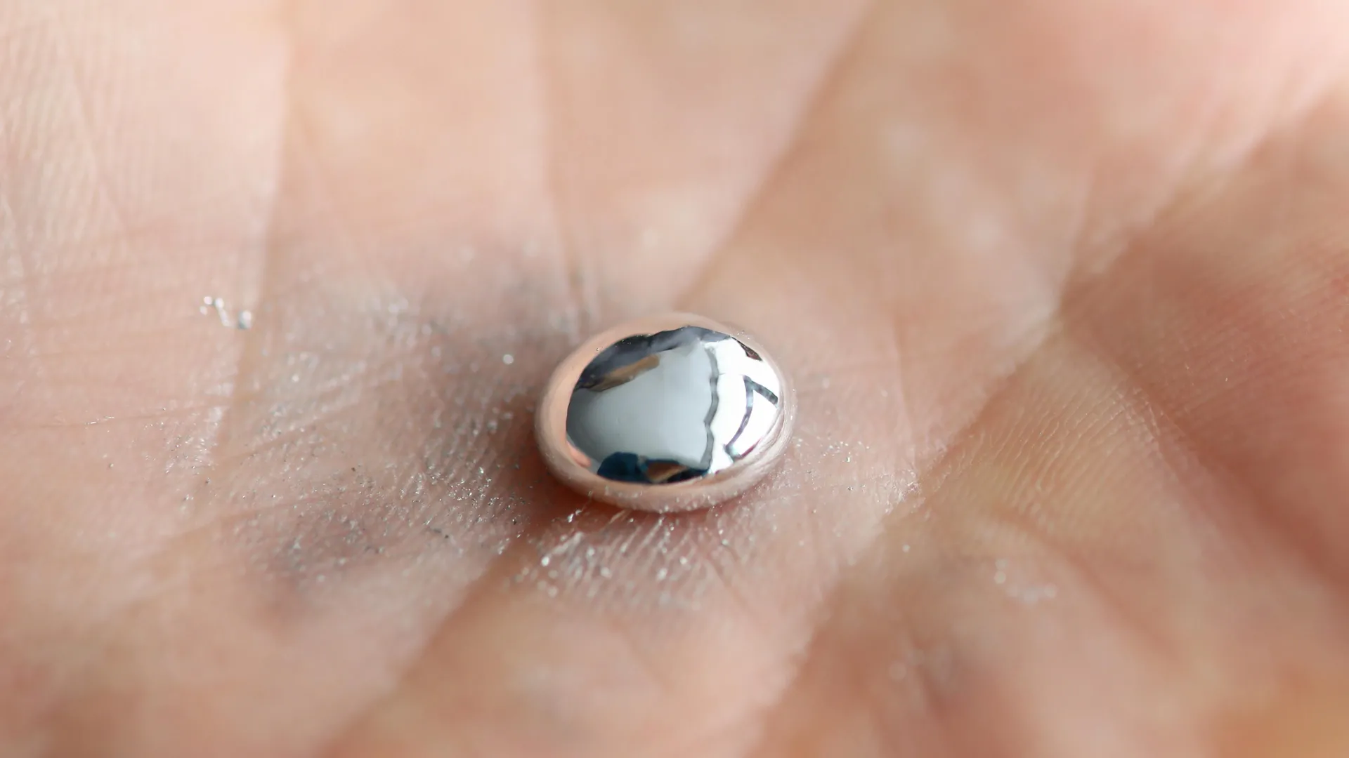
In a discovery that challenges the conventional understanding of semiconductor behavior, researchers at the University of California, Davis, have identified a remarkable "shape-shifting" property in halide perovskite crystals. According to a study published on March 3 in the journal Advanced Materials, these materials exhibit a phenomenon known as photostriction, where they undergo rapid and reversible physical deformation when exposed to light. This unique characteristic, which allows the crystals to expand and contract at the atomic level in response to illumination, could fundamentally alter the design of sensors, actuators, and light-controlled electronic components.
The research, led by Marina Leite, a professor of materials science and engineering at UC Davis, highlights a significant departure from the rigid nature of traditional semiconductors like silicon and gallium arsenide. While standard materials remain structurally static under light exposure, halide perovskites demonstrate a dynamic "smart" response. This discovery is expected to accelerate the development of switchable photonic devices, a field currently under intense scrutiny by global defense and technology agencies.
The Structural Blueprint: Understanding the ABX3 Framework
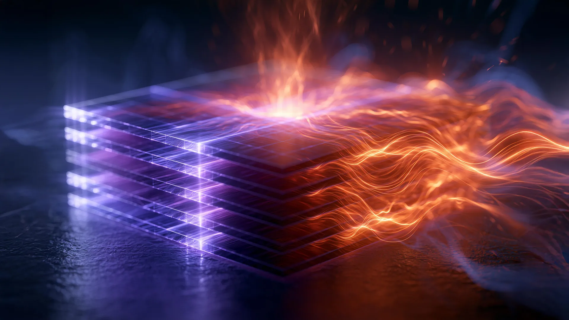
To appreciate the significance of the UC Davis findings, one must look at the unique atomic arrangement of perovskites. All materials in this class share a common crystalline structure designated as ABX3. In this configuration, a central atom (the "B" site, typically a metal like lead or tin) is surrounded by an octahedron—a shape resembling two pyramids joined at their bases—formed by six halogen atoms (the "X" site, such as iodine, bromine, or chlorine). This entire unit is nested within a larger cube, with atoms occupying each of the eight corners (the "A" site, often an organic molecule or a large inorganic cation).
This intricate geometry is what gives perovskites their versatile optoelectronic properties. For over a decade, scientists have primarily focused on their ability to convert sunlight into electricity, leading to a "perovskite revolution" in the solar industry. In 2009, perovskite solar cells had an efficiency of roughly 3.8%; today, that figure has soared to over 25%, rivaling established silicon technology. However, the UC Davis team shifted the focus from energy conversion to structural dynamics, investigating how the material itself moves when photons strike its surface.
Experimental Methodology and the Role of Photostriction
The investigation was a collaborative international effort, combining the synthesis expertise of researchers at ETH Zürich in Switzerland with the advanced characterization facilities at UC Davis. The crystals used in the study were meticulously produced by Bekir Turedi, Andrii Kanak, and Professor Maksym Kovalenko at ETH Zürich, ensuring the highest purity and structural integrity.
At UC Davis, graduate student Mansha Dubey conducted the primary experiments using the Advanced Materials Characterization and Testing (AMCaT) laboratory. The team employed a sophisticated setup where laser light was directed onto the perovskite crystals while their atomic structure was monitored in real-time using high-precision X-ray diffraction measurements.
The data revealed that when the laser light was activated, the internal lattice of the crystal shifted almost instantaneously. This phenomenon, photostriction, involves the conversion of light energy directly into mechanical strain. Unlike many other materials where such changes might be permanent or cause degradation, the perovskite crystals returned to their original dimensions as soon as the light source was removed. This cycle of expansion and contraction was found to be highly repeatable, suggesting a level of durability essential for commercial device applications.
A Tunable "Dimmer" Effect: Data and Observations
One of the most compelling aspects of the study is the discovery that the photostrictive response is not a simple binary (on/off) state. Instead, the researchers found that the degree of shape change can be precisely tuned.
Data from the experiments indicated two primary levers for controlling the material’s response:
- Light Intensity: As the brightness of the laser increased, the magnitude of the lattice displacement grew proportionally. This allows for a "scaled" response, similar to a dimmer switch on a light fixture, rather than a fixed mechanical toggle.
- Wavelength and Bandgap: By altering the chemical composition of the perovskites—specifically by swapping out different halogens in the "X" site—the researchers could change the material’s bandgap. The bandgap determines which colors of light the material absorbs. The study demonstrated that the structural response was most pronounced when the light frequency was above the material’s bandgap, providing a chemical pathway to customize devices for specific parts of the light spectrum, from ultraviolet to infrared.
"It is not a binary on/off effect; it can be a scaled response," Professor Leite explained. This granularity is a critical advantage for engineers looking to build precision instruments that require fine-tuned mechanical adjustments.
Comparative Analysis: Perovskites vs. Traditional Semiconductors
For decades, the semiconductor industry has been built on the back of silicon. Silicon is abundant, stable, and well-understood. However, silicon is also mechanically "dead" in response to light; it does not change its physical form. Gallium arsenide, another staple of the optoelectronics industry used in LEDs and high-frequency transistors, shares this rigidity.
Halide perovskites offer a stark contrast for several reasons:
- Mechanical Flexibility: The ability to undergo reversible strain makes them candidates for "soft" electronics and micro-electromechanical systems (MEMS).
- Cost-Effectiveness: Perovskites can be manufactured using solution-processing techniques, such as inkjet printing or spin-coating, at much lower temperatures than the energy-intensive Czochralski process used for silicon.
- Chemical Versatility: The "mix-and-match" nature of the ABX3 structure allows scientists to create thousands of different variations, each with unique electronic and mechanical signatures.
The UC Davis research suggests that while silicon will likely remain the king of pure data processing, perovskites will carve out a dominant niche in "active" devices that need to interact physically with their environment.
Timeline of the Research and Institutional Support
The path to the March 3 publication involved several years of interdisciplinary work and significant federal backing.
- Phase 1 (Synthesis): The crystals were developed at ETH Zürich, focusing on halide perovskites that could maintain stability under intense light exposure.
- Phase 2 (Testing): The materials were transported to the UC Davis AMCaT laboratory, where Dubey and Leite designed the laser-X-ray interface.
- Phase 3 (Analysis): Between 2023 and early 2024, the team analyzed the diffraction patterns to quantify the lattice strain and confirm the reversibility of the photostriction.
- Phase 4 (Publication): The findings were peer-reviewed and published in Advanced Materials in March 2024.
The project received substantial funding from the Defense Advanced Research Projects Agency (DARPA) through a program specifically aimed at developing materials for switchable photonic devices. These are devices that can route or modulate light signals on a chip, which is vital for the future of high-speed optical computing and secure communications. Additional support was provided by the National Science Foundation (NSF), which also funded the establishment of the AMCaT facility.
Future Implications: From Actuators to Light-Driven Robotics
The ability to control the shape of a material with light opens a vast array of technological possibilities. In the realm of telecommunications, light-controlled perovskite switches could replace electronic switches, reducing heat generation and increasing data transfer speeds.
In the field of robotics, the photostrictive effect could lead to the creation of "optical actuators"—tiny motors or limbs that move when illuminated. Because these components would not require wires or electricity to function, they could be used in environments where electromagnetic interference is a concern or where miniaturization makes wiring impossible.
Furthermore, the research has implications for the aerospace industry. Perovskites are known for their relative radiation hardness compared to silicon. A material that can both sense light and mechanically respond to it while surviving the harsh conditions of space would be invaluable for satellite sensors and autonomous deep-space probes.
Broader Impact and Industry Perspectives
While the discovery is currently at the fundamental research stage, the implications for the semiconductor industry are profound. Industry analysts suggest that the integration of "smart" materials like perovskites into existing manufacturing workflows could bridge the gap between traditional electronics and biological systems, which also rely on dynamic, responsive structures.
The research also highlights the growing importance of "materials by design." Instead of searching for naturally occurring minerals with specific properties, the UC Davis and ETH Zürich teams have demonstrated that we can engineer a material’s chemistry to achieve a desired mechanical outcome.
As the tech world moves toward the "Internet of Things" (IoT) and increasingly autonomous systems, the demand for sensors that are low-power and highly sensitive is skyrocketing. Perovskites, with their light-induced shape-shifting, offer a pathway to sensors that are powered and triggered by the very stimulus they are designed to detect.
Professor Leite and her team are expected to continue their investigation into the speed of these transitions. If the photostrictive response can be pushed to gigahertz frequencies, it could revolutionize how we think about signal processing, moving us away from electrons and toward a purely photonic future. For now, the UC Davis study serves as a definitive proof of concept that the future of semiconductors is not just about moving charge, but about moving matter itself.


Leave a Reply