

For decades, the photovoltaic industry has operated under a single, uncompromising mandate: purity is paramount. Silicon-based solar cells, which currently account for over 95% of the global market, require a level of material refinement that borders on the absolute. Even a single foreign atom among millions can disrupt the delicate flow of electrons, rendering a cell inefficient. However, a scientific revolution is underway, centered on a class of materials known as lead-halide perovskites. These materials defy the conventional laws of semiconductor physics by achieving remarkable efficiency despite being riddled with structural flaws and chemical impurities.
In a landmark study published in Nature Communications, researchers at the Institute of Science and Technology Austria (ISTA) have finally decoded the mechanism behind this "perovskite paradox." The team, led by Dmytro Rak and Zhanybek Alpichshev, has identified a hidden network of internal "highways" that allow electrical charges to bypass defects and travel vast distances. This discovery not only solves a decade-long mystery in materials science but also provides a roadmap for the next generation of low-cost, high-performance renewable energy technology.
The Rise of the Perovskite Challenger
The story of lead-halide perovskites is one of the most rapid ascents in the history of science. While the perovskite crystal structure was first discovered in 1839 by Gustav Rose and named after Russian mineralogist Lev Perovski, the specific lead-halide variants remained a laboratory curiosity for over a century. It wasn’t until 2009 that Tsutomu Kojima and his colleagues at Toin University of Yokohama first integrated them into a solar cell, achieving a modest power conversion efficiency (PCE) of 3.8%.
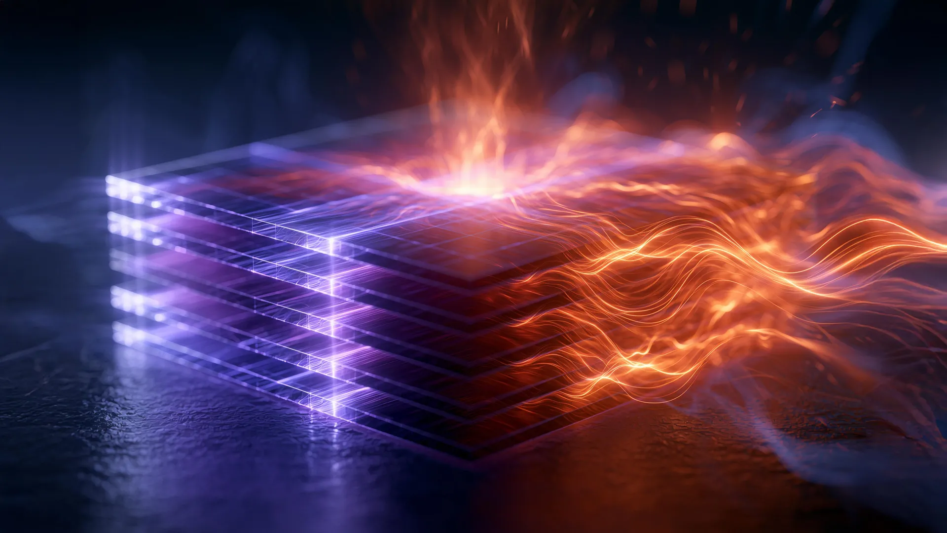
In the fifteen years since that initial experiment, perovskite efficiency has skyrocketed to over 26%, a trajectory that took silicon technology more than half a century to achieve. What makes this rise even more startling is the method of production. Silicon wafers must be grown in high-temperature vacuum environments using the Czochralski process, a costly and energy-intensive procedure. In contrast, perovskites can be printed or "spin-coated" from liquid solutions at room temperature, much like ink on paper.
Despite this ease of manufacture, scientists remained baffled. Under a microscope, these solution-processed materials look like a chaotic mess of crystalline grains and defects. In any other semiconductor, such "messiness" would trap electrical charges, causing them to lose energy as heat. Yet, in perovskites, the charges move with an uncanny freedom.
The Mechanics of Charge Separation
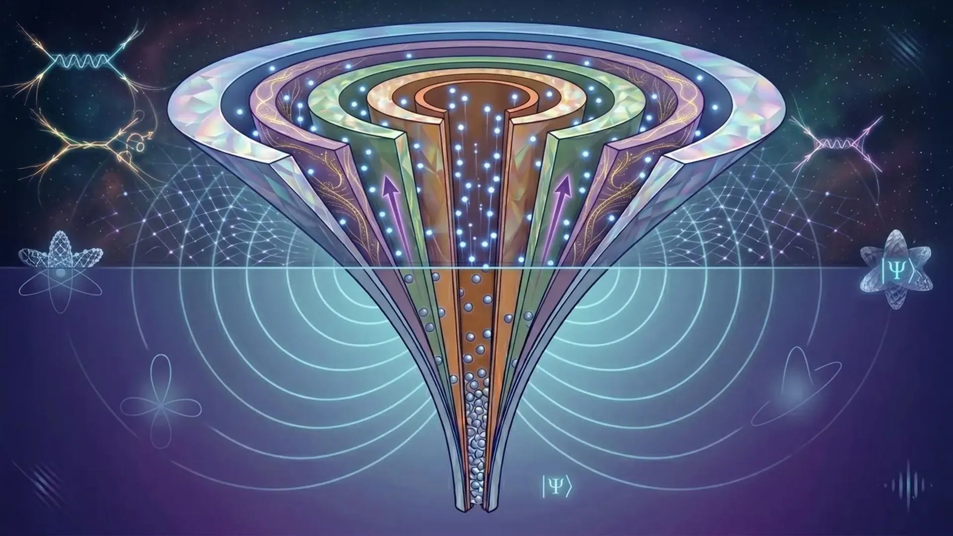
To understand the ISTA breakthrough, one must first look at how a solar cell functions at the subatomic level. When a photon of sunlight strikes a semiconductor, it provides enough energy to knock an electron loose, leaving behind a positively charged vacancy known as a "hole." For electricity to be generated, this electron and hole must be separated and guided to opposite electrodes.
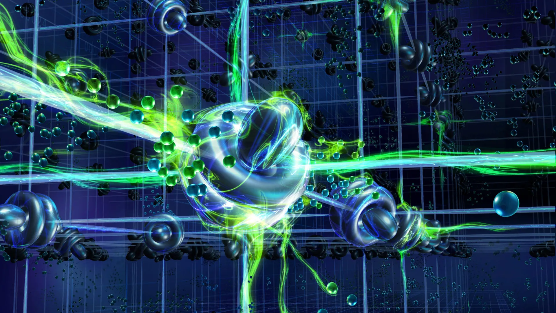
In most materials, electrons and holes are naturally attracted to one another, forming a bound state called an exciton. If they meet, they "recombine" and the energy is lost. The challenge for researchers has been explaining why, in flawed perovskite crystals, these charges remain separated for so long and travel so far—often hundreds of microns, which is a massive distance relative to the atomic scale.
The ISTA team hypothesized that there must be an internal force pulling these charges apart. Using advanced nonlinear optical techniques, Rak and Alpichshev injected charges deep into the bulk of the material. They observed a spontaneous electrical current flowing in a specific direction without any external voltage. This confirmed the presence of internal electric fields, but the question remained: where were these fields coming from?
Mapping the Internal Highways
The researchers discovered that the source of these fields lies in "domain walls." These are thin boundaries within the crystal where the alignment of the atoms shifts slightly. While these walls were previously thought to be minor defects, the ISTA study reveals they are the secret to the material’s success.
"Our findings suggest that these domain walls are not just passive boundaries," explains Zhanybek Alpichshev. "They act as specialized pathways. When an electron and a hole are created near a wall, the local electric field pulls them in opposite directions—placing the electron on one side of the wall and the hole on the other. Because they are physically separated by the wall, they cannot recombine. They are then free to zip along these ‘highways’ toward the electrodes."
To prove this, the team had to visualize structures that exist deep within the opaque crystal. Dmytro Rak developed a pioneering technique inspired by medical imaging. By introducing silver ions into the perovskite, the researchers found that the ions naturally migrated toward these domain walls. Once the ions were chemically reduced to metallic silver, they formed a visible map of the internal network.
"This is essentially angiography for crystals," says Alpichshev. "Just as doctors use dyes to see blood vessels in living tissue, we used silver to reveal the hidden architecture that moves charges through the perovskite."
Comparative Data: Silicon vs. Perovskites
The implications of this discovery are best understood by comparing the technical requirements and performance metrics of the two competing technologies.
| Feature | Silicon Solar Cells | Perovskite Solar Cells |
|---|---|---|
| Material Purity | 99.9999% (Electronic Grade) | Low (Defect-tolerant) |
| Manufacturing Temp | ~1,400°C | <150°C |
| Energy Payback Time | 1–2 years | <3 months |
| Theoretical Efficiency | ~29% | ~33% |
| Flexibility | Rigid/Brittle | Flexible/Lightweight |
| Primary Limitation | High Capex / Rigid Structure | Long-term Stability |
The data highlights a significant shift in the economic landscape of solar energy. Because perovskites can be manufactured with far less energy and lower-grade materials, the "energy payback time"—the time a panel must operate to produce the energy required to make it—is drastically reduced.
Industry Reactions and the Road to Commercialization
The ISTA study has resonated throughout the materials science community. Independent experts suggest that understanding the "highway" system of domain walls could finally allow engineers to move past the trial-and-error phase of perovskite development.
"For years, we’ve been throwing different chemical additives at perovskites to see what sticks," says Dr. Elena Rossi, a photovoltaic researcher not involved in the study. "The ISTA team has given us a structural blueprint. If we can learn to engineer these domain walls—controlling their density and orientation—we could potentially push efficiencies beyond the 30% mark in the near future."
However, challenges remain. While the ISTA research explains the efficiency, the industry is still grappling with the issue of longevity. Lead-halide perovskites are sensitive to moisture and heat, often degrading within a few years, whereas silicon panels are guaranteed for 25 years. Furthermore, the presence of lead, albeit in small amounts, raises environmental concerns that must be addressed through robust recycling programs.
Chronology of Perovskite Development
- 1839: Discovery of the perovskite mineral (CaTiO3) in the Ural Mountains.
- 1978: First synthesis of lead-halide perovskites.
- 2009: First use in a solar cell (3.8% efficiency).
- 2012: Breakthrough discovery of solid-state perovskite cells, increasing stability and efficiency to over 10%.
- 2017: Perovskite-silicon tandem cells begin to emerge, promising to break the 30% efficiency barrier.
- 2024: ISTA researchers publish the "domain wall" theory in Nature Communications, providing the first unified physical explanation for the material’s efficiency.
Broader Impact and Future Implications
The discovery of charge highways in perovskites extends beyond solar panels. These materials are also showing immense potential in the field of optoelectronics. Because they are highly efficient at converting electricity back into light, they are being developed for next-generation LEDs that are more vibrant and energy-efficient than current OLED technology.
Additionally, the ISTA team’s observation of "quantum coherence at room temperature" within these materials suggests they could play a role in quantum computing or advanced sensors. The ability of a relatively "dirty" and inexpensive material to maintain quantum states at room temperature is a phenomenon that could redefine our approach to quantum materials.
As the world races toward net-zero carbon emissions, the need for scalable, cheap, and efficient energy sources has never been more urgent. Silicon has brought us far, but it may be reaching its physical and economic limits. By unlocking the secrets of the perovskite paradox, the ISTA researchers have provided the scientific foundation needed to transition from the laboratory to the factory floor.
The next step for the research team will be to investigate how these domain walls can be manipulated through external stressors or chemical doping. If the "highways" can be optimized, the result would be a solar cell that is not only cheaper to produce than silicon but also significantly more powerful. The era of "imperfect" semiconductors has arrived, and it promises to be brighter than the era of purity that preceded it.


Leave a Reply