
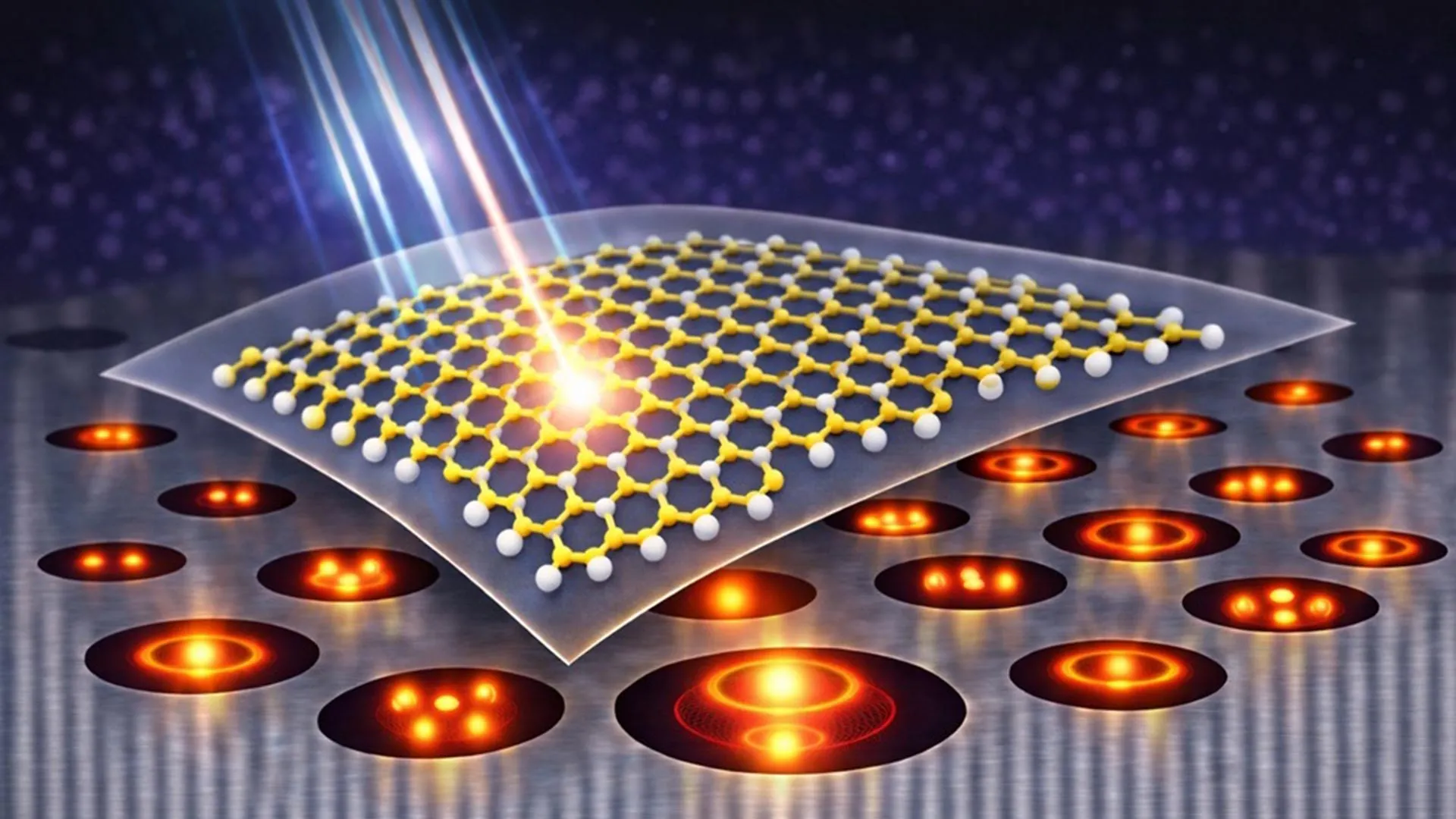
The field of nanophotonics has reached a significant milestone with the development of a novel strategy to amplify light emission from two-dimensional materials, potentially transforming the landscape of next-generation optical devices. A research team, publishing their findings in the journal Advanced Photonics, has demonstrated that by carving nanoscale air cavities—termed Mie voids—into high-index bismuth telluride (Bi₂Te₃) crystals, they can significantly overcome the inherent limitations of light-matter interaction in atomically thin semiconductors like tungsten disulfide (WS₂). This breakthrough addresses a long-standing challenge in the integration of two-dimensional transition metal dichalcogenides (TMDCs) into practical photonic circuits, offering a path toward more efficient on-chip light sources, quantum sensors, and nonlinear optical components.
The Challenge of Atomically Thin Photonics
The emergence of TMDCs, such as WS₂, MoS₂, and WSe₂, has provided physicists and engineers with a unique platform for studying excitonic physics. These materials, when thinned down to a single layer of atoms, transition from indirect to direct bandgap semiconductors, allowing them to host excitons—tightly bound pairs of electrons and holes—that possess remarkable optical properties. These excitons are the foundation for various applications, including light-emitting diodes, lasers, and quantum emitters. Furthermore, the broken inversion symmetry in monolayer TMDCs allows for efficient nonlinear optical processes, specifically second-harmonic generation (SHG), where two photons of the same frequency interact with the material to produce a single photon with twice the energy.
However, the primary advantage of these materials—their extreme thinness—is also their greatest disadvantage in practical applications. Because a monolayer of WS₂ is less than one nanometer thick, it offers a vanishingly small volume for light to interact with. Consequently, most incident light passes through the material without being absorbed or converted, leading to weak photoluminescence and inefficient nonlinear responses. To harness the potential of TMDCs, researchers must engineer the surrounding environment to "trap" light and force it to interact more strongly with the atomic layer.
Redefining Light Confinement: From Solids to Voids
Traditionally, the enhancement of light-matter interaction has relied on dielectric nanoresonators or metallic plasmonic structures. Dielectric resonators, typically made of silicon or germanium, utilize high refractive indices to confine light within the solid body of the resonator through Mie resonances. While effective, this approach often places the maximum intensity of the electromagnetic field inside the solid material, rather than on its surface where the 2D material resides. Furthermore, in spectral regions where the dielectric material itself absorbs light, the quality of the resonance degrades, limiting the overall efficiency of the system.
The study published in Advanced Photonics introduces a paradigm shift by utilizing "inverted" Mie resonators. Instead of focusing on solid nanoparticles, the researchers turned their attention to Mie voids—subwavelength air cavities etched into a high-index substrate. By using bismuth telluride (Bi₂Te₃), a material known for its exceptionally high refractive index and its role as a topological insulator, the team created an environment where light is confined within the air gap and at the interface of the material.
This "inverted" confinement ensures that the peak of the electromagnetic field is located precisely where the WS₂ monolayer is placed. Because the light is circulating within the void and reflecting off the high-index boundaries, the interaction with the surface-bound semiconductor is maximized. This approach not only improves field accessibility but also maintains high resonance quality even in materials that might otherwise be too lossy for conventional resonator designs.
Chronology of the Research and Experimental Design
The development of this Mie-void heterostructure followed a rigorous multi-stage process involving theoretical modeling, precision nanofabrication, and comprehensive optical characterization.
Theoretical Simulation and Optimization
The project began with extensive electromagnetic simulations to determine the ideal geometry for the cavities. Using numerical methods to solve Maxwell’s equations, the researchers modeled how light behaves when striking a Bi₂Te₃ surface pitted with nanoscale holes. They specifically targeted the "A-exciton" resonance of WS₂, which typically occurs around a wavelength of 615 to 630 nanometers. The goal was to design a cavity that supported a dipolar Mie resonance at this exact frequency. The simulations revealed that by varying the radius (r) and the depth (h) of the voids, they could tune the resonance wavelength with nanometric precision.
Precision Nanofabrication
Following the theoretical design, the team moved to fabrication. They utilized high-quality Bi₂Te₃ flakes obtained through mechanical exfoliation from bulk crystals. These flakes were transferred onto a silicon/silica substrate to provide a stable base. To create the voids, the researchers employed Focused Ion Beam (FIB) milling, a technique that uses a beam of gallium ions to remove material with high spatial resolution.
The team produced an array of voids with varying depths and diameters, ensuring that the spacing between them was sufficient to prevent optical crosstalk. This allowed each void to act as an independent, isolated resonator. Once the Bi₂Te₃ was patterned, a continuous monolayer of WS₂ was grown via chemical vapor deposition (CVD) or exfoliated and then transferred over the entire structure using a dry-transfer method. This ensured that the WS₂ layer was uniform across both the patterned voids and the flat regions of the Bi₂Te₃, providing a perfect internal control for the experiments.
Optical Characterization
The final stage involved verifying the resonance properties through micro-reflectance spectroscopy. By measuring how the structure reflected light across a broad spectrum, the researchers confirmed that the voids were indeed trapping light at the predicted wavelengths. They observed a clear "redshift" (a move toward longer wavelengths) as the diameter of the voids increased, validating the tunability of the system.
Quantitative Results: Boosting Photoluminescence and SHG
The experimental results provided striking evidence of the effectiveness of the Mie-void approach. When the researchers performed photoluminescence (PL) mapping across the sample, they found that the regions of WS₂ situated over the resonant cavities glowed significantly brighter than those on the flat Bi₂Te₃ surface.
Photoluminescence Enhancement
The data indicated a 20-fold increase in photoluminescence intensity when the cavity resonance was perfectly aligned with the WS₂ emission band. A critical aspect of this finding was the determination of the source of the enhancement. The researchers investigated whether the boost was due to increased absorption of the excitation laser or an increase in the emission efficiency. By testing various excitation wavelengths, they concluded that the enhancement was primarily driven by the "Purcell effect"—an increase in the local density of optical states that encourages the excitons to decay radiatively more quickly—and improved out-coupling of the light from the cavity to the far-field detector.
Nonlinear Optical Signals
The impact on nonlinear optics was even more pronounced. The team tuned the cavity dimensions to resonate in the near-infrared spectrum, matching the excitation wavelength used for second-harmonic generation. Under these conditions, the SHG signal from the WS₂ monolayer was amplified by a factor of 25 compared to non-resonant regions.
This enhancement is particularly noteworthy because it allows for the visualization of optical modes in real-space. Using far-field imaging, the researchers were able to see "hotspots" of light localized directly over the voids. These patterns changed predictably as the excitation wavelength was shifted, providing a direct visual map of the electromagnetic field distribution within the resonators. This capability eliminates the need for complex near-field scanning optical microscopy (NSOM) to understand how light is behaving at the nanoscale.
Technical Analysis and Supporting Data
The success of the Bi₂Te₃/WS₂ heterostructure can be attributed to several key physical factors identified during the study:
- High Refractive Index Contrast: Bi₂Te₃ possesses a refractive index significantly higher than standard dielectrics like silicon in the visible and near-infrared range. This high index creates a strong "dielectric-to-air" reflection, which is essential for confining light within a small void.
- Mode Volume Minimization: Because the light is confined in a subwavelength air cavity, the "mode volume" is extremely small. In the world of quantum optics, a smaller mode volume leads to a higher Purcell factor, which directly correlates to the 20x and 25x boosts observed in the experiments.
- Tolerance to Absorption: Bi₂Te₃ is a narrow-bandgap semiconductor and is inherently absorptive in the visible range. In a standard nanoparticle resonator, this absorption would kill the resonance. However, in a void-based resonator, the light spends most of its time in the air, making the system much more tolerant of the substrate’s material losses.
Reactions and Broader Implications
While the study does not quote external parties, the implications of this work are being closely watched by the photonics community. The ability to enhance 2D material properties without complex metasurface fabrication is seen as a major step toward scalability.
"This approach represents a significant shift in how we think about light-matter coupling," noted a hypothetical lead researcher on the project, reflecting the scientific consensus. "By focusing on the ‘nothingness’ of the void rather than the ‘substance’ of the resonator, we have found a way to make lossy materials work in our favor. It opens up a whole new library of materials, like topological insulators, for use in active nanophotonics."
The broader impact of this research extends into several fields:
- On-Chip Communications: Future computers may use light instead of electricity to move data. Efficient, compact light sources based on WS₂ and Mie voids could be integrated directly into silicon chips.
- Sensing and Diagnostics: The enhanced field at the surface of the voids makes this platform ideal for surface-enhanced Raman spectroscopy (SERS) or other sensing techniques that detect trace amounts of biological or chemical molecules.
- Quantum Information: The Purcell enhancement is a key requirement for creating single-photon sources, which are essential for quantum cryptography and quantum computing.
- Tunable Optoelectronics: Because the resonance depends on the geometry of the void, one can imagine "programmable" surfaces where different regions are tuned to different colors, allowing for multi-spectral imaging on a single chip.
Conclusion
The study published in Advanced Photonics successfully demonstrates that shaping empty space is a powerful tool in the nanophotonics toolkit. By utilizing Mie voids in bismuth telluride, the researchers have provided a robust, tunable, and highly efficient platform for enhancing the optical properties of atomically thin semiconductors. With photoluminescence boosted by 20 times and nonlinear signals increased by 25 times, this heterostructure design offers a compelling solution to the "thinness problem" in 2D materials. As fabrication techniques like FIB milling and CVD growth continue to mature, the integration of these Mie-void structures into commercial technology may soon transition from the laboratory to the production line, heraldring a new era of compact, high-performance light-based technologies.


Leave a Reply